- 您現(xiàn)在的位置:買賣IC網 > PDF目錄379312 > MC68HLC908JK3E (Motorola, Inc.) Microcontrollers PDF資料下載
參數(shù)資料
| 型號: | MC68HLC908JK3E |
| 廠商: | Motorola, Inc. |
| 英文描述: | Microcontrollers |
| 中文描述: | 微控制器 |
| 文件頁數(shù): | 164/226頁 |
| 文件大?。?/td> | 1549K |
| 代理商: | MC68HLC908JK3E |
第1頁第2頁第3頁第4頁第5頁第6頁第7頁第8頁第9頁第10頁第11頁第12頁第13頁第14頁第15頁第16頁第17頁第18頁第19頁第20頁第21頁第22頁第23頁第24頁第25頁第26頁第27頁第28頁第29頁第30頁第31頁第32頁第33頁第34頁第35頁第36頁第37頁第38頁第39頁第40頁第41頁第42頁第43頁第44頁第45頁第46頁第47頁第48頁第49頁第50頁第51頁第52頁第53頁第54頁第55頁第56頁第57頁第58頁第59頁第60頁第61頁第62頁第63頁第64頁第65頁第66頁第67頁第68頁第69頁第70頁第71頁第72頁第73頁第74頁第75頁第76頁第77頁第78頁第79頁第80頁第81頁第82頁第83頁第84頁第85頁第86頁第87頁第88頁第89頁第90頁第91頁第92頁第93頁第94頁第95頁第96頁第97頁第98頁第99頁第100頁第101頁第102頁第103頁第104頁第105頁第106頁第107頁第108頁第109頁第110頁第111頁第112頁第113頁第114頁第115頁第116頁第117頁第118頁第119頁第120頁第121頁第122頁第123頁第124頁第125頁第126頁第127頁第128頁第129頁第130頁第131頁第132頁第133頁第134頁第135頁第136頁第137頁第138頁第139頁第140頁第141頁第142頁第143頁第144頁第145頁第146頁第147頁第148頁第149頁第150頁第151頁第152頁第153頁第154頁第155頁第156頁第157頁第158頁第159頁第160頁第161頁第162頁第163頁當前第164頁第165頁第166頁第167頁第168頁第169頁第170頁第171頁第172頁第173頁第174頁第175頁第176頁第177頁第178頁第179頁第180頁第181頁第182頁第183頁第184頁第185頁第186頁第187頁第188頁第189頁第190頁第191頁第192頁第193頁第194頁第195頁第196頁第197頁第198頁第199頁第200頁第201頁第202頁第203頁第204頁第205頁第206頁第207頁第208頁第209頁第210頁第211頁第212頁第213頁第214頁第215頁第216頁第217頁第218頁第219頁第220頁第221頁第222頁第223頁第224頁第225頁第226頁
Input/Output (I/O) Ports
Technical Data
MC68H(R)C908JL3E/JK3E/JK1E
—
Rev. 2.0
164
Input/Output (I/O) Ports
MOTOROLA
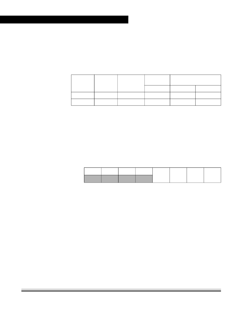
When DDRDx is a logic 1, reading address $0003 reads the PTDx data
latch. When DDRDx is a logic 0, reading address $0003 reads the
voltage level on the pin. The data latch can always be written, regardless
of the state of its data direction bit.
Table 12-4
summarizes the operation
of the port D pins.
Table 12-4. Port D Pin Functions
12.5.3 Port D Control Register (PDCR)
The port D control register enables/disables the pull-up resistor and
slow-edge high current capability of pins PTD6 and PTD7.
SLOWDx — Slow Edge Enable
The SLOWD6 and SLOWD7 bits enable the Slow-edge, open-drain,
high current output (25mA sink) of port pins PTD6 and PTD7
respectively. DDRDx bit is not affected by SLOWDx.
1 = Slow edge enabled; pin is open-drain output
0 = Slow edge disabled; pin is push-pull
PTDPUx — Pull-up Enable
The PTDPU6 and PTDPU7 bits enable the 5k
pull-up on PTD6 and
PTD7 respectively, regardless the status of DDRDx bit.
1 = Enable 5k
pull-up
0 = Disable 5k
pull-up
DDRD
Bit
PTD Bit
I/O Pin
Mode
Accesses
to DDRD
Accesses to PTD
Read/Write
Read
Write
PTD[7:0]
(3)
0
X
(1)
Notes
:
1. X = don’t care.
2. Hi-Z = high impedance.
3. Writing affects data register, but does not affect the input.
Input, Hi-Z
(2)
DDRD[7:0]
Pin
1
X
Output
DDRD[7:0]
Pin
PTD[7:0]
Address:
$000A
Bit 7
6
5
4
3
2
1
Bit 0
Read:
0
0
0
0
SLOWD7 SLOWD6 PTDPU7
PTDPU6
Write:
Reset:
0
0
0
0
0
0
0
0
Figure 12-12. Port D Control Register (PDCR)
相關PDF資料 |
PDF描述 |
|---|---|
| MC68HLC908JL3E | Microcontrollers |
| MC68HRC908JK3E | Microcontrollers |
| MC68HRC908JL3E | Microcontrollers |
| MC68HRC98JK1ECDW | CA06COME22-23PBF80 |
| MC68HRC98JK1ECP | CA-BAYONET |
相關代理商/技術參數(shù) |
參數(shù)描述 |
|---|---|
| MC68HLC908QT1CFQ | 制造商:Rochester Electronics LLC 功能描述:- Bulk |
| MC68HLC908QT4CDW | 制造商:Rochester Electronics LLC 功能描述:- Bulk |
| MC68HLC908QT4CFQ | 制造商:Rochester Electronics LLC 功能描述:- Bulk |
| MC68HLC908QY1CDW | 制造商:Rochester Electronics LLC 功能描述:LOW V-1.5K FLASH W/O ADC - Bulk |
| MC68HLC908QY1DT | 制造商:Rochester Electronics LLC 功能描述:- Tape and Reel |
發(fā)布緊急采購,3分鐘左右您將得到回復。