- 您現(xiàn)在的位置:買賣IC網(wǎng) > PDF目錄379305 > MC143421FU (MOTOROLA INC) PCI Bus Interface PDF資料下載
參數(shù)資料
| 型號: | MC143421FU |
| 廠商: | MOTOROLA INC |
| 元件分類: | 總線控制器 |
| 英文描述: | PCI Bus Interface |
| 中文描述: | PCI BUS CONTROLLER, PQFP100 |
| 封裝: | QFP-100 |
| 文件頁數(shù): | 4/11頁 |
| 文件大?。?/td> | 189K |
| 代理商: | MC143421FU |
MC143421
4
MOTOROLA
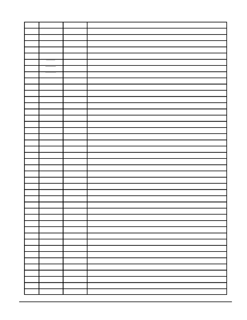
Table 1. Pin Descriptions (continued)
43
AD[4]
I/O
PCI Bus Multiplexed Address and Data
44
AD[3]
I/O
PCI Bus Multiplexed Address and Data
45
AD[2]
I/O
PCI Bus Multiplexed Address and Data
46
GND
Ground
47
AD[1]
I/O
PCI Bus Multiplexed Address and Data
48
AD[0]
I/O
PCI Bus Multiplexed Address and Data
49
READ
O
PIB Read Strobe
50
WRITE
O
PIB Write Strobe
51
RESET
O
PIB Reset — Generated by PCI Reset
52
GND
Ground
53
VCC
ha[3]
Power 5 V
54
O
PIB Address — Subsystem ID (Sampled at Reset)
55
ha[2]
O
PIB Address — Subsystem ID (Sampled at Reset)
56
ha[1]
O
PIB Address — Subsystem ID (Sampled at Reset)
57
ha[0]
O
PIB Address — Subsystem ID (Sampled at Reset)
58
GND
Ground
59
hd[7]
I/O
PIB Data — Subvender ID (Sampled at Reset)
60
hd[6]
I/O
PIB Data — Subvender ID (Sampled at Reset)
61
hd[5]
I/O
PIB Data — Subvender ID (Sampled at Reset)
62
hd[4]
I/O
PIB Data — Subvender ID (Sampled at Reset)
63
hd[3]
I/O
PIB Data — Subvender ID (Sampled at Reset)
64
hd[2]
I/O
PIB Data — Subvender ID (Sampled at Reset)
65
VCC
GND
Power 5 V
66
Ground
67
hd[1]
I/O
PIB Data — Subvender ID (Sampled at Reset)
68
hd[0]
I/O
PIB Data — Subvender ID (Sampled at Reset)
69
aux[7]
I/O
PIB Programmable General Purpose I/O (See Figure 1)
70
aux[6]
I/O
PIB Programmable General Purpose I/O (See Figure 1)
71
aux[5]
I/O
PIB Programmable General Purpose I/O (See Figure 1)
72
aux[4]
I/O
PIB Programmable General Purpose I/O (See Figure 1)
73
GND
Ground
74
PME#
OC
PCI Power Management Event
75
NC
No Connect
76
NC
No Connect
77
NC
No Connect (Or 10 k Resistor Pull–Down — See Device Class Section)
78
NC
No Connect (Or 10 k Resistor Pull–Down — See Device Class Section)
79
VCC
aux[3]
Power 5 V
80
I/O
PIB Programmable General Purpose I/O (See Figure 1)
81
aux[2]
I/O
PIB Programmable General Purpose I/O (See Figure 1)
82
aux[1]
I/O
PIB Programmable General Purpose I/O (See Figure 1)
83
aux[0]
I/O
PIB Programmable General Purpose I/O (See Figure 1)
84
GND
Ground
85
INTA#
O
PCI Interrupt
86
RST#
I
PCI Device Reset
相關(guān)PDF資料 |
PDF描述 |
|---|---|
| MC14495DW1 | HEXADECIMAL-TO-SEVEN SEGMENT LATCH/DECODER LED DRIVER |
| MC14495 | Digital Signal Processor 196-CFP -55 to 125 |
| MC14495P1 | HEXADECIMAL-TO-SEVEN SEGMENT LATCH/DECODER LED DRIVER |
| MC14497P | Digital Signal Processor,Military Known Good Die 0-XCEPT -55 to 125 |
| MC14499 | Digital Signal Processor,Military Known Good Die 0-XCEPT -55 to 125 |
相關(guān)代理商/技術(shù)參數(shù) |
參數(shù)描述 |
|---|---|
| MC1435G | 制造商:Motorola Inc 功能描述: |
| MC1436C6 | 制造商:Motorola Inc 功能描述: |
| MC1436CD | 制造商:Rochester Electronics LLC 功能描述:- Bulk |
| MC1436CDR2 | 制造商:Rochester Electronics LLC 功能描述:- Bulk |
| MC1436D | 制造商:Rochester Electronics LLC 功能描述:- Bulk |
發(fā)布緊急采購,3分鐘左右您將得到回復。