- 您現(xiàn)在的位置:買賣IC網(wǎng) > PDF目錄379301 > MC10E196 (ON SEMICONDUCTOR) PROGRAMMABLE DELAY CHIP PDF資料下載
參數(shù)資料
| 型號: | MC10E196 |
| 廠商: | ON SEMICONDUCTOR |
| 英文描述: | PROGRAMMABLE DELAY CHIP |
| 中文描述: | 可編程延時芯片 |
| 文件頁數(shù): | 3/7頁 |
| 文件大小: | 148K |
| 代理商: | MC10E196 |
MC10E196 MC100E196
2–3
MOTOROLA
ECLinPS and ECLinPS Lite
DL140 — Rev 4
AC CHARACTERISTICS
(continued) (VEE = VEE(min) to VEE(max); VCC = VCCO = GND)
0
°
C
25
°
C
85
°
C
Symbol
Characteristic
Min
Typ
Max
Min
Typ
Max
Min
Typ
Max
Unit
Notes
ts
Setup Time
D to LEN
D to IN
EN to IN
200
800
200
0
200
800
200
0
200
800
200
0
ps
2
3
th
Hold Time
LEN to D
IN to EN
500
0
250
500
0
250
500
0
250
ps
4
tR
Release Time
EN to IN
SET MAX to LEN
SET MIN to LEN
300
800
800
300
800
800
300
800
800
ps
5
tjit
tr
tf
Jitter
<5.0
<5.0
<5.0
ps
8
Output Rise/Fall Time
20–80% (Q)
20–80% (CASCADE)
125
300
225
450
325
650
125
300
225
450
325
650
125
300
225
450
325
650
ps
1. Duty cycle skew guaranteed only for differential operation measured from the cross point of the input to the cross point of the output.
2. This setup time defines the amount of time prior to the input signal the delay tap of the device must be set.
3. This setup time is the minimum time that EN must be asserted prior to the next transition of IN/IN to prevent an output response greater than
±
75 mV to that IN/IN transition.
4. This hold time is the minimum time that EN must remain asserted after a negative going IN or positive going IN to prevent an output response
greater than
±
75 mV to that IN/IN
transition.
5. This release time is the minimum time that EN must be deasserted prior to the next IN/IN transition to ensure an output response that meets
the specified IN to Q propagation delay and
transition times.
6. Specification limits represent the amount of delay added with the assertion of each individual delay control pin. The various combinations of
asserted delay control inputs will typically
realize D0 resolution steps across the specified programmable range.
7. The linearity specification guarantees to which delay control input the programmable steps will be monotonic (i.e. increasing delay steps for
increasing binary counts on the control inputs Dn). Typically the device will be monotonic to the D0 input, however under worst case conditions
and process variation, delays could decrease slightly with increasing binary counts when the D0 input is the LSB. With the D1 input as the LSB
the device is guaranteed to be monotonic over all specified environmental conditions and process variation.
8. The jitter of the device is less than what can be measured without resorting to very tedious and specialized measurement techniques.
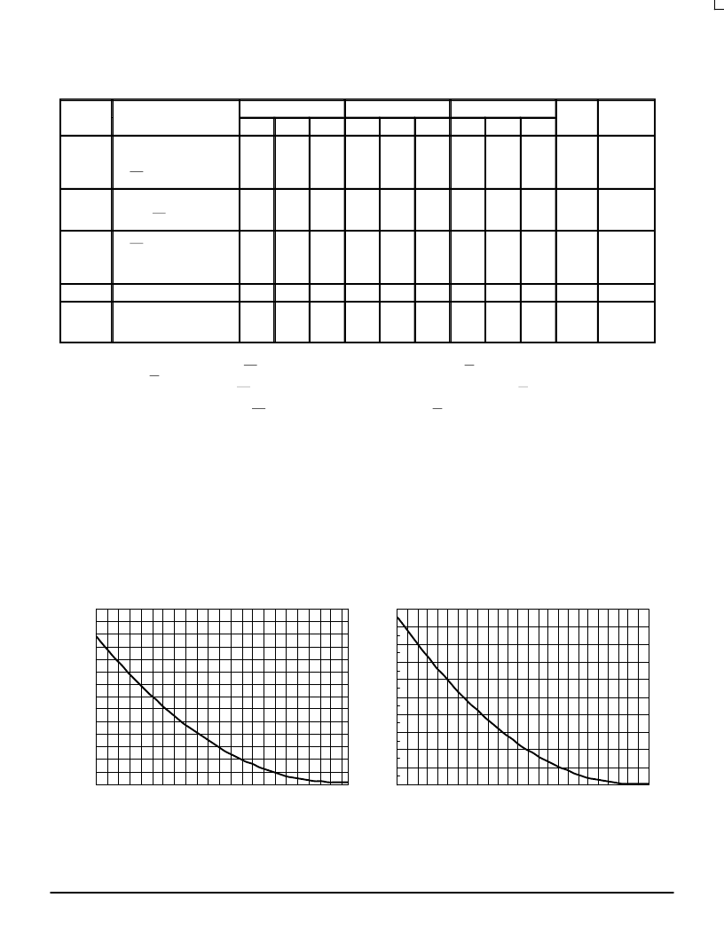
ANALOG INPUT CHARACTERISTICS
Ftune = VCC to VEE
FTUNE VOLTAGE (V)
140
120
100
80
60
40
20
0
–4.5
–3.5
–2.5
–1.5
–0.5
P
Propagation Delay versus Ftune Voltage
(100E196)
FTUNE VOLTAGE (V)
100
90
80
70
60
50
40
30
20
10
0
–5
–4
–3
–2
–1
0
P
Propagation Delay versus Ftune Voltage
(10E196)
相關(guān)PDF資料 |
PDF描述 |
|---|---|
| MC100E196FN | PROGRAMMABLE DELAY CHIP |
| MC10E404FN | QUAD DIFFERENTIAL AND/NAND |
| MC10E404 | QUAD DIFFERENTIAL AND/NAND |
| MC100E404FN | QUAD DIFFERENTIAL AND/NAND |
| MC10E411FN | 0.345A, 2.7-5.5V Dual (1In/2Out) Hi-Side MOSFET, Fault Report, Act-High Enable 8-SOIC 0 to 85 |
相關(guān)代理商/技術(shù)參數(shù) |
參數(shù)描述 |
|---|---|
| MC10E196 B29M WAF | 制造商:ON Semiconductor 功能描述: |
| MC10E196FN | 功能描述:延遲線/計時元素 5V ECL Programmable RoHS:否 制造商:Micrel 功能:Active Programmable Delay Line 傳播延遲時間:1000 ps 工作溫度范圍: 封裝 / 箱體:QFN-24 封裝:Tube |
| MC10E196FNG | 功能描述:延遲線/計時元素 5V ECL Programmable Delay RoHS:否 制造商:Micrel 功能:Active Programmable Delay Line 傳播延遲時間:1000 ps 工作溫度范圍: 封裝 / 箱體:QFN-24 封裝:Tube |
| MC10E196FNR2 | 功能描述:延遲線/計時元素 5V ECL Programmable RoHS:否 制造商:Micrel 功能:Active Programmable Delay Line 傳播延遲時間:1000 ps 工作溫度范圍: 封裝 / 箱體:QFN-24 封裝:Tube |
| MC10E196FNR2G | 功能描述:延遲線/計時元素 5V ECL Programmable Delay RoHS:否 制造商:Micrel 功能:Active Programmable Delay Line 傳播延遲時間:1000 ps 工作溫度范圍: 封裝 / 箱體:QFN-24 封裝:Tube |
發(fā)布緊急采購,3分鐘左右您將得到回復(fù)。