- 您現(xiàn)在的位置:買(mǎi)賣(mài)IC網(wǎng) > PDF目錄65794 > LB1813MS DISK DRIVE MOTOR CONTROLLER, PDSO36 PDF資料下載
參數(shù)資料
| 型號(hào): | LB1813MS |
| 元件分類(lèi): | 運(yùn)動(dòng)控制電子 |
| 英文描述: | DISK DRIVE MOTOR CONTROLLER, PDSO36 |
| 封裝: | 0.375 INCH, MFP-36 |
| 文件頁(yè)數(shù): | 2/8頁(yè) |
| 文件大小: | 115K |
| 代理商: | LB1813MS |
LB1813MS
No.A0868-2/8
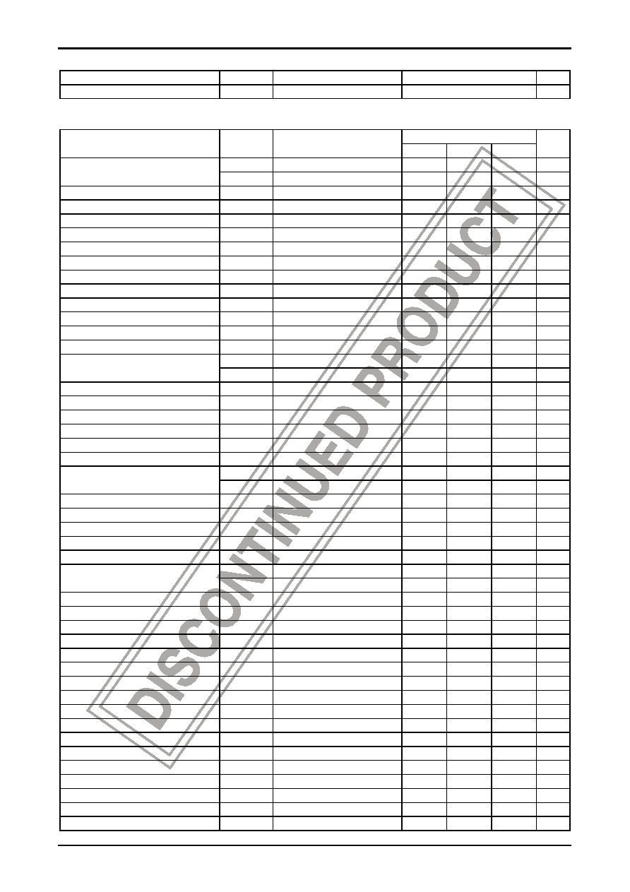
Allowable Operating Conditions at Ta = 25
°C
Parameter
Symbol
Conditions
Ratings
Unit
Suppiy voltage
VCC
4.2 to 6.5
V
Electrical Characteristics at Ta
= 25°C, VCC = 5V
Ratings
Parameter
Symbol
Conditions
min
typ
max
Unit
ICCO1
VCC = 5.0V (Stop)
0.4
mA
Current drain
ICC1
VCC = 5.0V (Steady)
20
30
mA
Time changeover bias current
ISL
0.4
mA
Time changeover input voltage1
VSLL
0
0.8
V
Time changeover input voltage2
VSLH
2.0
VCC
V
S/S bias current
IS/S
0.1
mA
S/S start voltage
VS/S
0
0.8
V
S/S stop voltage
VS/S
2.0
VCC
V
Hall-effect bias amplifier input current
IHB
20
μA
In-phase input voltage range
Vh
2.2
VCC-0.7
V
Differential input voltage range
Vdif
70
200
mVp-p
Input offset voltage
Vho
*
±10
mV
Hall-effect output voltage
VH
IH = 5mA
1.5
1.8
V
Leak current
IHL
Stop
±10
μA
Vsat1
IO = 0.35A, VCC = 4.2V
1.2
1.4
V
Output saturation voltage
(sink plus source)
Vsat2
IO = 0.70A, VCC = 4.2V
1.5
2.0
V
Output leak current
IOL
±10
mA
current limiter
Vref1
0.27
0.30
0.33
V
Control amplifier voltage gain
GC
-6
dB
Voltage gain phase differential
ΔGC
±1dB
Integrated amplifier internal reference voltage
Vref2
VCC/2
V
Integrated amplifier bias current
lib
±1
μA
Vi+
Ii = -0.5mA with reference of Vref2
0.75
V
Integrated output voltage amplitude
Vi-
Ii = 0.5mA with reference of Vref2
-1.4
V
Gain band width
*
1000
kHz
FG amplifier input voltage range
VFG
5
100
mVp-p
FG amplifier voltage gain
GFG
60
dB
FG amplifier input offset
VFG0
±10
mV
FG amplifier internal reference voltage
VFGB
2.20
2.50
2.80
V
ΔVsh1
High
→ Low *
25
mV
Schmitt hysteresis width
ΔVsh2
Low
→ High *
25
mV
Schmitt input operation level
Vsh
1
VCC-1
V
Speed disk recount number
N
1042
Disk recount out low level voltage
VDL
ID = -0.5mA
0.3
V
Disk recount out high level voltage
VDH
ID = 0.5mA
VCC-0.4
V
Disk recount out leak current
ID1
±1.0
μA
Disk recount operation frequency
FD
*
1.1
MHz
Oscillation range
FOSC
*
1.1
MHz
Index bias current
IIDB
±10
μA
In-phase input voltage range
VID
1.5
VCC-0.5
V
Hysteresis setting current range
IIDO
5
10
15
μA
Index output low level voltage
VIDL
VID = 5V
0.4
V
Index output high level voltage
VIDH
VID = 5V
4.5
V
Brake-down voltage
VDLDC
VID = 5V
2.50
V
Delay output low level voltage
VDLL
VID = 5V
0.4
V
Delay output high level voltage
VDLH
VID = 5V
4.5
V
Thermal shutdown operating temperature
TSD
*
150
180
°C
Hysteresis temperature
ΔTSD
*
40
°C
Note : *) Marked values are guaranteed by the design itself and therefore do not require measurement.
相關(guān)PDF資料 |
PDF描述 |
|---|---|
| LB1820 | BRUSHLESS DC MOTOR CONTROLLER, 2.5 A, PDIP28 |
| LB1831M | BRUSH DC MOTOR CONTROLLER, PDSO16 |
| LB1838JM | STEPPER MOTOR CONTROLLER, PDSO14 |
| LB1838JM | STEPPER MOTOR CONTROLLER, PDSO14 |
| LB1840M | STEPPER MOTOR CONTROLLER, 0.25 A, PDSO14 |
相關(guān)代理商/技術(shù)參數(shù) |
參數(shù)描述 |
|---|---|
| LB1814M | 制造商:SANYO 制造商全稱(chēng):Sanyo Semicon Device 功能描述:LB1814M |
| LB1816 | 制造商:SANYO 制造商全稱(chēng):Sanyo Semicon Device 功能描述:LB1816 |
| LB1817M | 制造商:SANYO 制造商全稱(chēng):Sanyo Semicon Device 功能描述:FDD Spindle Motor Driver |
| LB1817W | 制造商:未知廠(chǎng)家 制造商全稱(chēng):未知廠(chǎng)家 功能描述:DC Motor Controller/Driver |
| LB1820 | 制造商:SANYO 制造商全稱(chēng):Sanyo Semicon Device 功能描述:Office Automation-Use 3-Phase Brushless Motor Driver |
發(fā)布緊急采購(gòu),3分鐘左右您將得到回復(fù)。