- 您現在的位置:買賣IC網 > PDF目錄65794 > LB11825M BRUSHLESS DC MOTOR CONTROLLER, 3 A, PDSO14 PDF資料下載
參數資料
| 型號: | LB11825M |
| 元件分類: | 運動控制電子 |
| 英文描述: | BRUSHLESS DC MOTOR CONTROLLER, 3 A, PDSO14 |
| 封裝: | 0.225 ICNH, MFP-14 |
| 文件頁數: | 7/8頁 |
| 文件大小: | 96K |
| 代理商: | LB11825M |
LB11825M
No.7108-7/8
LB11825M Functional Description
1. Basic operation
This IC multiplies the frequency of the clock signals that have been input from the external source, and outputs them.
The multiplied frequency can be calculated using the following formula.
fOUT = fCLK × internal frequency (where fOUT : multiplied output frequency, fCLK : input clock frequency)
The maximum input clock frequency is 16kHz, and the maximum multiplied output frequency is 1MHz. The IC must
therefore be used within these parameters.
It is assumed that LB11825M will be used in conjunction with LB11822, LB11826, LB11827 or other motor driver
IC. Its use in conjunction with any of these ICs makes it possible to exercise variable-speed control over motors using
the clock signals with a frequency that corresponds to the FG frequency of the motors.
2. VCC power supply
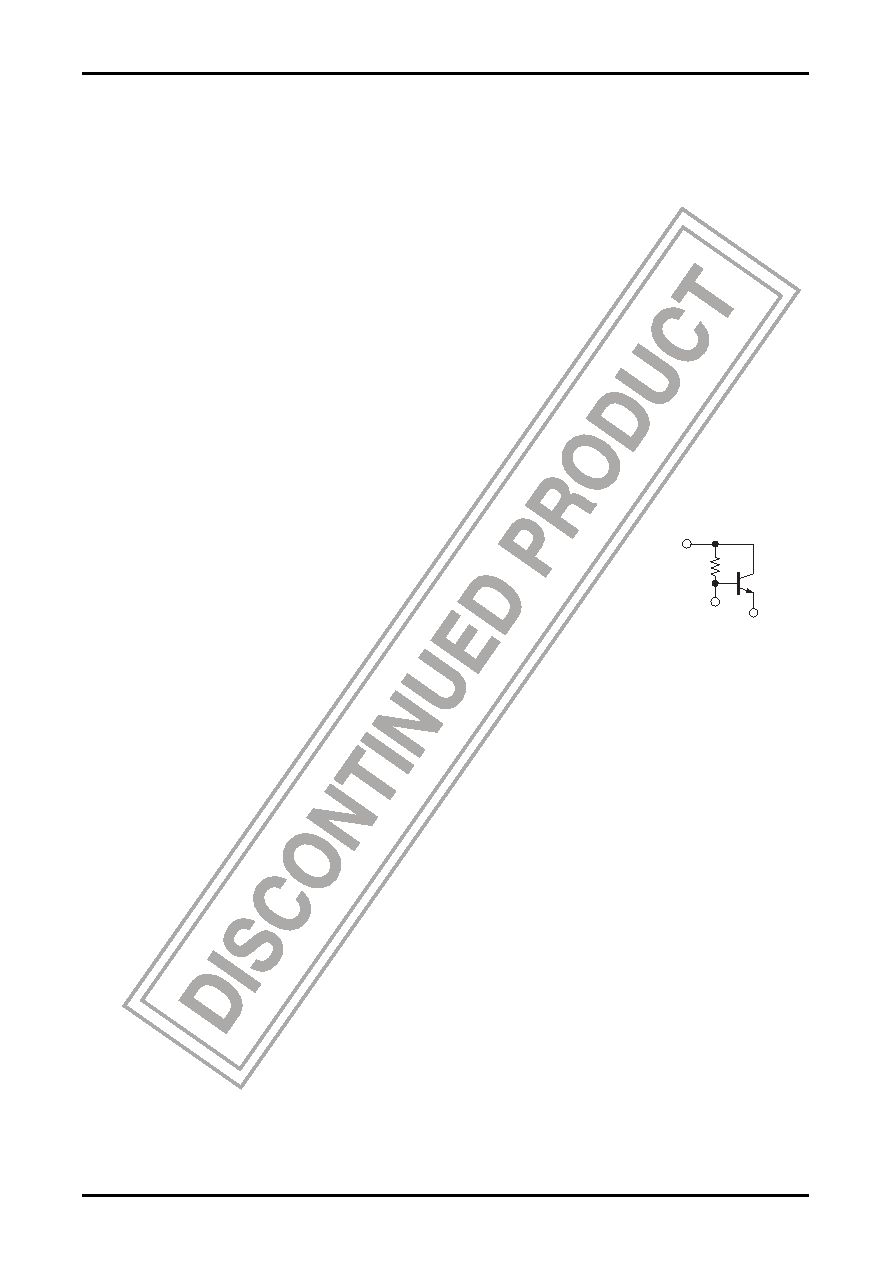
When LB11825M is used in conjunction with LB11822, LB11826, LB11827 or other motor driver IC, the VREG
output (5V) of the driver IC can be used as the VCC power supply of the LB11825M IC. However, in cases where
the heat generated by the ICs must be reduced or where the range of variation in the multiplied output frequency is to
be increased, a voltage of approximately 6.4V can be supplied to the VCC pin of LB11825M by connecting an
external resistor and NPN transistor as shown in the figure on the right to the VREG pin (7.1V shunt regulator) of
LB11825M.
Since fluctuations in the VCC supply voltage will adversely affect the stability of the multiplied output frequency,
the frequency must be stabilized by connecting a capacitor between the VCC pin and ground.
3. External resistor and capacitor constants for FIL pin
The capacitor between the FIL pin and ground is provided to suppress the voltage ripple
of the FIL pin. Therefore, even when the input clock frequency is low, the capacitance of
this capacitor must be selected in such a way that the FIL pin voltage is sufficiently
smoothed.
Furthermore, connecting a resistor and capacitor in series between the FIL pin and ground
shortens the convergence time (i.e., the time taken until the multiplied output frequency
stabilizes) of the FIL pin voltage when the input clock frequency is switched. This means
that the resistor and capacitor constants must be set in accordance with the required
convergence time.
4. External resistor and capacitor constants for R pin, C pin
The maximum variation range for the multiplied output frequency when 5V is used as the VCC power supply is
about
× 4. To increase this range, the constants of the external resistance (R) for the R pin and external capacitance
(C) for the C pin must be determined with reference given to the following steps, since they are determined by the
maximum multiplied output frequency value (fOUT1) to be set, and by the minimum VCC power supply fluctuation
value (VCC1).
(1) Using the following formula, calculate R1 and C1, and decide on the values of R and C so that R is equal to or
less than R1, and C is equal to or less than C1, even when the resistor and capacitor fluctuations (including the
temperature characteristics, etc.) are factored in.
R1 = (VCC1 - 2.2V)/280μA
C1 = (280
μA /0.7V) × (1/fOUT1) × 0.7
(2) The minimum value (fOUT2) of the multiplied output frequency that can be set with the constants of R and C as
determined in step (1) is calculated using the following formula with R2 and C2 serving as the minimum values
based on the fluctuations (including the temperature characteristics, etc.) of R and C, respectively. This means
that the variation range in the multiplied output frequency that can be set will be fOUT1 to fOUT2.
fOUT2 = 0.41/(R2 × C2)
Continued on next page.
24V
To VREG
To VCC
(Approx. 6.4V)
相關PDF資料 |
PDF描述 |
|---|---|
| LB11867RV | BRUSHLESS DC MOTOR CONTROLLER, 0.02 A, PDSO16 |
| LB11961 | BRUSHLESS DC MOTOR CONTROLLER, 1 A, PDSO16 |
| LB11961 | BRUSHLESS DC MOTOR CONTROLLER, 1 A, PDSO16 |
| LB11967V | BRUSHLESS DC MOTOR CONTROLLER, 0.05 A, PDSO20 |
| LB11967V | BRUSHLESS DC MOTOR CONTROLLER, 0.6 A, PDSO10 |
相關代理商/技術參數 |
參數描述 |
|---|---|
| LB11826 | 制造商:SANYO 制造商全稱:Sanyo Semicon Device 功能描述:For OA Products Three-Phase Brushless Motor Driver |
| LB11826_08 | 制造商:SANYO 制造商全稱:Sanyo Semicon Device 功能描述:For OA Products Three-Phase Brushless Motor Driver |
| LB11826-E | 功能描述:馬達/運動/點火控制器和驅動器 RoHS:否 制造商:STMicroelectronics 產品:Stepper Motor Controllers / Drivers 類型:2 Phase Stepper Motor Driver 工作電源電壓:8 V to 45 V 電源電流:0.5 mA 工作溫度:- 25 C to + 125 C 安裝風格:SMD/SMT 封裝 / 箱體:HTSSOP-28 封裝:Tube |
| LB11827 | 制造商:SANYO 制造商全稱:Sanyo Semicon Device 功能描述:Three-Phase Brushless Motor Driver for OA Products |
| LB11847 | 制造商:SANYO 制造商全稱:Sanyo Semicon Device 功能描述:PWM Current Control Type Stepping Motor Driver |
發(fā)布緊急采購,3分鐘左右您將得到回復。