- 您現(xiàn)在的位置:買賣IC網(wǎng) > PDF目錄374361 > KM718BV87 (SAMSUNG SEMICONDUCTOR CO. LTD.) 64Kx18-Bit Synchronous SRAM(64Kx18位同步靜態(tài) RAM) PDF資料下載
參數(shù)資料
| 型號(hào): | KM718BV87 |
| 廠商: | SAMSUNG SEMICONDUCTOR CO. LTD. |
| 英文描述: | 64Kx18-Bit Synchronous SRAM(64Kx18位同步靜態(tài) RAM) |
| 中文描述: | 64Kx18位同步SRAM(64Kx18位同步靜態(tài)內(nèi)存) |
| 文件頁(yè)數(shù): | 2/12頁(yè) |
| 文件大小: | 276K |
| 代理商: | KM718BV87 |
PRELIMINARY
KM718BV87
64Kx18 Synchronous SRAM
- 2 -
Rev 1.1
April 1997
FAST ACCESS TIMES
Parameter
Symbol
t
CYC
t
CD
t
OE
-9
15
9
5
-10
17
10
5
-12
20
12
6
Unit
ns
ns
ns
Cycle Time
Clock Access Time
Output Enable Access Time
64Kx18-Bit Synchronous Burst SRAM
FEATURES
The KM718BV87 is a 1,179,648 bits Synchronous Static Ran-
dom Access Memory designed to support zero wait state perfor-
mance with advanced i486/Pentium address pipelining.
When CS is high, ADSP is blocked to control singles.
It is organized as 65,536 words of 18bits and integrates address
and control registers, a 2-bit burst address counter and high out-
put drive circuitry onto a single integrated circuit for reduced
components count implementations of high performance cache
RAM applications.
Write cycles are internally self-timed and synchronous.
The self-timed write feature eliminates complex off chip write
pulse shaping logic, simplifying the cache design and further
reducing the component count.
Burst cycle can be initiated with either the address status pro-
cessor(ADSP) or address status cache controller(ADSC) inputs.
Subsequent burst addresses are generated internally in the sys-
tem
′
s burst sequence and are controlled by the burst address
advance(ADV) input.
The KM718BV87 is implemented with SAMSUNG
′
s high perfor-
mance BiCMOS technology and is available in a 52pin PLCC
package. Multiple power and ground pins are utilized to mini-
mize ground bounce.
GENERAL DESCRIPTION
ü
Synchronous Operation.
ü
On-Chip Address Counter.
ü
Self-Timed Write Cycle.
ü
On-Chip Address and Control Registers.
ü
Single 3.3V
±
5% Power Supply.
ü
Byte Writable Function.
ü
Asynchronous Output Enable Control.
ü
ADSP, ADSC, ADV Burst Control Pins.
ü
TTL-Level Three-State Output.
ü
5V I/O Compatible.
ü
52-Pin PLCC Package.
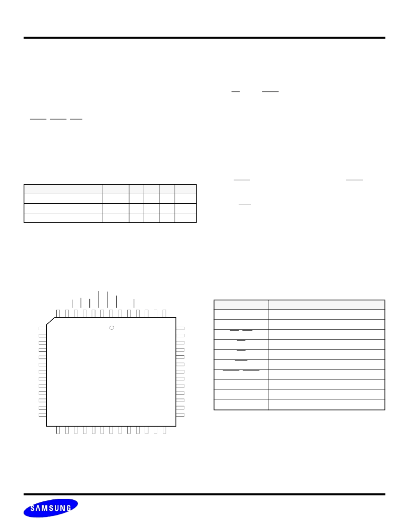
PIN NAME
Pin Name
A
0
- A
15
K
LW, UW
CS
OE
ADV
ADSP, ADSC
I/O
0
~I/O
17
V
CC
V
SS
Pin Function
Address Inputs
Clock
Write Enable
Chip Selects
Output Enable
Burst Address Advance
Address Status
Data Inputs/Outputs
+3.3V Power Supple
Ground
8
9
10
11
12
13
14
15
16
17
18
19
20
52-PLCC-SQ
I/O
9
I/O
10
V
CC
V
SS
I/O
11
I/O
12
I/O
13
I/O
14
V
SS
V
CC
I/O
15
I/O
16
I/O
17
46
45
44
43
42
41
40
39
38
37
36
35
34
I/O
8
I/O
7
I/O
6
V
CC
V
SS
I/O
5
I/O
4
I/O
3
I/O
2
V
SS
V
CC
I/O
1
I/O
0
7
6
5
4
3
2
1 52 51 50 49 48 47
A
6
A
7
C
A
A
A
K
O
33
32
31
30
29
28
27
26
25
24
23
22
V
C
V
S
A
0
A
1
A
2
A
3
A
4
A
5
21
A
1
A
1
A
1
A
1
A
1
U
L
A
8
A
9
A
1
PIN CONFIGURATION
(TOP VIEW)
相關(guān)PDF資料 |
PDF描述 |
|---|---|
| KM718V687 | 64Kx18 Synchronous SRAM(64Kx18位同步靜態(tài) RAM) |
| KM718V787 | 128Kx18 Synchronous SRAM(128Kx18位同步靜態(tài) RAM) |
| KM718V789A | 128Kx18 Synchronous SRAM(128Kx18位同步靜態(tài) RAM) |
| KM718V789 | 128Kx18 Synchronous SRAM(128Kx18位同步靜態(tài) RAM) |
| KM718V889 | 256Kx18 Synchronous SRAM(256Kx18位同步靜態(tài) RAM) |
相關(guān)代理商/技術(shù)參數(shù) |
參數(shù)描述 |
|---|---|
| KM718FV4021 | 制造商:SAMSUNG 制造商全稱:Samsung semiconductor 功能描述:128Kx36 & 256Kx18 Synchronous Pipelined SRAM |
| KM718FV4021H-5 | 制造商:SAMSUNG 制造商全稱:Samsung semiconductor 功能描述:128Kx36 & 256Kx18 Synchronous Pipelined SRAM |
| KM718FV4021H-6 | 制造商:SAMSUNG 制造商全稱:Samsung semiconductor 功能描述:128Kx36 & 256Kx18 Synchronous Pipelined SRAM |
| KM718FV4021H-7 | 制造商:SAMSUNG 制造商全稱:Samsung semiconductor 功能描述:128Kx36 & 256Kx18 Synchronous Pipelined SRAM |
| KM718N | 制造商:FRONTIER 制造商全稱:Frontier Electronics. 功能描述:10mm Adjustable Unshielded IFT Coils |
發(fā)布緊急采購(gòu),3分鐘左右您將得到回復(fù)。