- 您現(xiàn)在的位置:買賣IC網(wǎng) > PDF目錄374275 > K4J52324QC-BJ12 (SAMSUNG SEMICONDUCTOR CO. LTD.) 512Mbit GDDR3 SDRAM PDF資料下載
參數(shù)資料
| 型號: | K4J52324QC-BJ12 |
| 廠商: | SAMSUNG SEMICONDUCTOR CO. LTD. |
| 英文描述: | 512Mbit GDDR3 SDRAM |
| 中文描述: | 512MB的GDDR3 SDRAM的 |
| 文件頁數(shù): | 42/57頁 |
| 文件大小: | 1246K |
| 代理商: | K4J52324QC-BJ12 |
第1頁第2頁第3頁第4頁第5頁第6頁第7頁第8頁第9頁第10頁第11頁第12頁第13頁第14頁第15頁第16頁第17頁第18頁第19頁第20頁第21頁第22頁第23頁第24頁第25頁第26頁第27頁第28頁第29頁第30頁第31頁第32頁第33頁第34頁第35頁第36頁第37頁第38頁第39頁第40頁第41頁當(dāng)前第42頁第43頁第44頁第45頁第46頁第47頁第48頁第49頁第50頁第51頁第52頁第53頁第54頁第55頁第56頁第57頁
- 42 -
Rev 1.0 (Mar 2005)
512M GDDR3 SDRAM
K4J52324QC-B
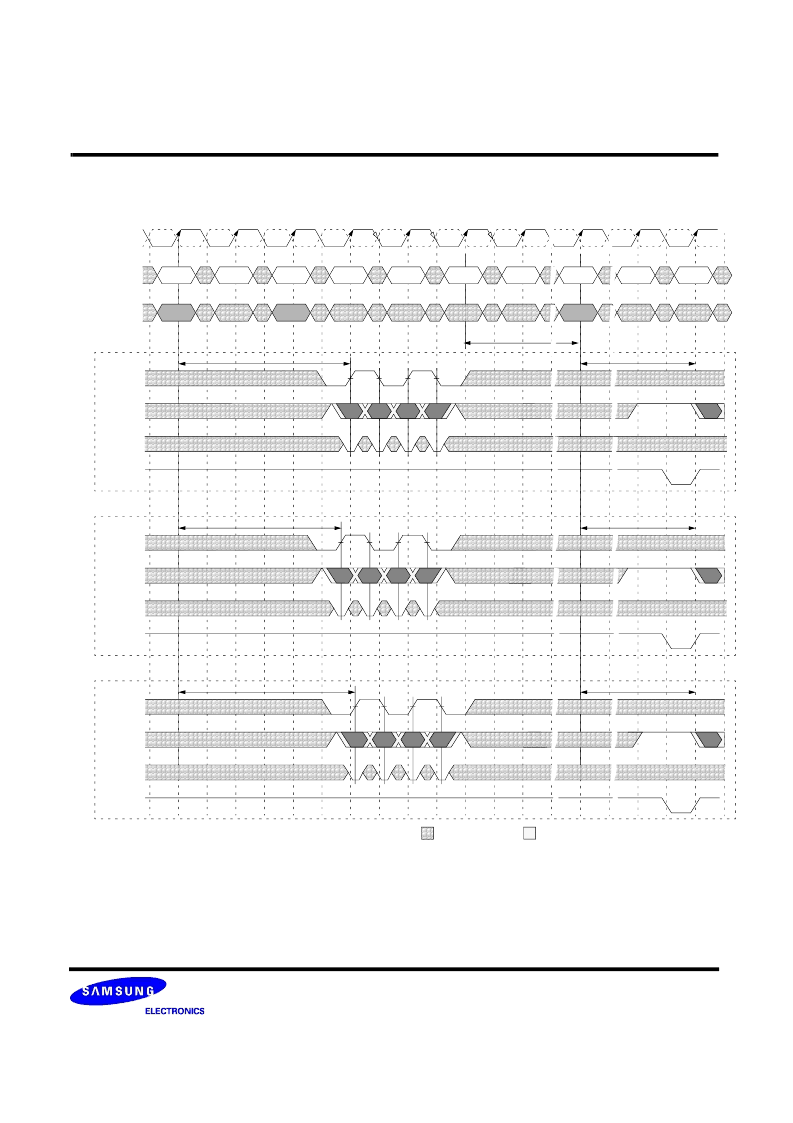
WRITE to READ
DON’T CARE
TRANSITIONING DATA
NOTE
:
NOP
NOP
WRITE
NOP
NOP
WRITE
T0
T1
T3
T3n
T4
T5
/CK
CK
COMMAND
ADDRESS
Bank
Col b
t
DQSS
NOP
T4n
T6
DQ
DM
WDQS
T2
T10
READ
DI
b
Bank
Col b
T18
T19
NOP
NOP
t
DQSS
(NOM)
Bank a.
Col n
CL = 8
RDQS
t
DQSS
DQ
DM
WDQS
DI
b
DI
n
t
DQSS
(MIN)
CL = 8
RDQS
DI
n
t
DQSS
DQ
DM
WDQS
DI
b
DI
n
t
DQSS
(MAX)
CL = 8
RDQS
tCDLR = 5
T19n
1. DI
b
= data-in for column
b
.
2. Three subsequent elements of data-in the programmed order following DI
b.
3. A burst of 4 is shown.
4. t
CDLR
is referenced from the first positive CK edge after the last data-in pair.
5. The READ and WRITE commands are to the same device. However, the READ and WRITE commands may be
to different devices, in which case t
CDLR
is not required and the READ command could be applied earlier.
6. A8 is LOW with the WRITE command (auto precharge is disabled).
7. WRITE latency is set to 3
~~
~~
~~
~~
~~
~~
~~
~~
~~
~~
~
~~
~~
~~
~~
~~
~~
~~
~~
~~
~~
~~
~~
~~
~~
~~
~~
相關(guān)PDF資料 |
PDF描述 |
|---|---|
| K4J52324QC-BJ14 | 512Mbit GDDR3 SDRAM |
| K4M281633F | 2M x 16Bit x 4 Banks Mobile SDRAM in 54FBGA |
| K4M281633F-C | 2M x 16Bit x 4 Banks Mobile SDRAM in 54FBGA |
| K4M281633F-F1L | 2M x 16Bit x 4 Banks Mobile SDRAM in 54FBGA |
| K4M281633F-G | 2M x 16Bit x 4 Banks Mobile SDRAM in 54FBGA |
相關(guān)代理商/技術(shù)參數(shù) |
參數(shù)描述 |
|---|---|
| K4J52324QC-BJ14 | 制造商:SAMSUNG 制造商全稱:Samsung semiconductor 功能描述:512Mbit GDDR3 SDRAM |
| K4J52324QE-BC12000 | 制造商:Samsung Semiconductor 功能描述: |
| K4J52324QE-BC14000 | 制造商:Samsung Semiconductor 功能描述: |
| K4J52324QE-BC16000 | 制造商:Samsung Semiconductor 功能描述:GDDR3 SDRAM X32 BOC - Trays |
| K4J52324QH-AC14000 | 制造商:Samsung Semiconductor 功能描述:GDDR3 SDRAM X32 BOC LEAD PART 10W - Trays |
發(fā)布緊急采購,3分鐘左右您將得到回復(fù)。