- 您現(xiàn)在的位置:買賣IC網(wǎng) > PDF目錄374275 > K4J52324QC-BC20 (SAMSUNG SEMICONDUCTOR CO. LTD.) 512Mbit GDDR3 SDRAM PDF資料下載
參數(shù)資料
| 型號: | K4J52324QC-BC20 |
| 廠商: | SAMSUNG SEMICONDUCTOR CO. LTD. |
| 英文描述: | 512Mbit GDDR3 SDRAM |
| 中文描述: | 512MB的GDDR3 SDRAM的 |
| 文件頁數(shù): | 28/57頁 |
| 文件大小: | 1246K |
| 代理商: | K4J52324QC-BC20 |
第1頁第2頁第3頁第4頁第5頁第6頁第7頁第8頁第9頁第10頁第11頁第12頁第13頁第14頁第15頁第16頁第17頁第18頁第19頁第20頁第21頁第22頁第23頁第24頁第25頁第26頁第27頁當(dāng)前第28頁第29頁第30頁第31頁第32頁第33頁第34頁第35頁第36頁第37頁第38頁第39頁第40頁第41頁第42頁第43頁第44頁第45頁第46頁第47頁第48頁第49頁第50頁第51頁第52頁第53頁第54頁第55頁第56頁第57頁
- 28 -
Rev 1.0 (Mar 2005)
512M GDDR3 SDRAM
K4J52324QC-B
OPERATIONS
BANK/ROW ACTIVATION
Before any READ or WRITE commands can be issued to a banks within the GDDR3 SDRAM,
a row in that bank must be "opened." This is accomplished via the ACTIVE command, which
selects both the bank and the row to be activated.
After a row is opened with an ACTIVE command, a READ or WRITE command may be issued
to that row, subject to the t
RCD
specification. t
RCD(min)
should be divided by the clock period
and rounded up to the next whole number to determine the earliest clock edge after the
ACTIVE command in which a READ or WRITE command can be entered. For example, a t
RCD
specification of 16ns with a 800MHz clock (1.25ns period) results in 12.8 clocks rounded to 13.
This is reflected in below figure, which covers any case where 12<t
RCD(min)
/t
CK
≤
13.
The same procedure is used to convert other specification limits from tome units to clock
cycles).
A subsequent ACTIVE command to a different row in the same bank can only be issued after
the previous active row has been "closed"(precharged). The minimum time interval between
successive ACTIVE commads to the same bank is defined by t
RC
.
A subsequent ACTIVE command to another bank can be issued while the first bank is being
accessed, which results in a reduction of total row access overhead. The minimum time inter-
val between successive ACTIVE commands to different banks is defined by t
RRD
.
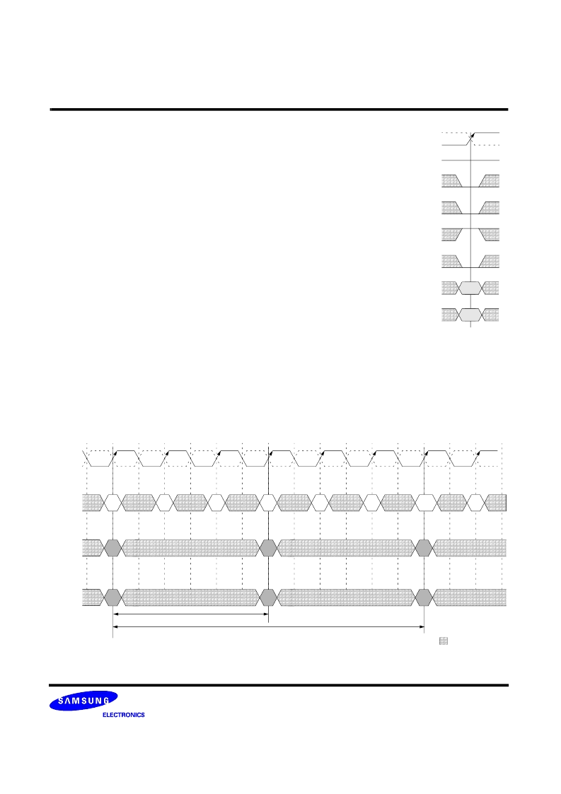
/CK
CK
RA
CKE
/CS
/RAS
/CAS
/WE
A0-A11
BA0,1,2
HIGH
BA
RA = Row Address
BA = Bank Address
Activating a Specific Row
in a Specific Bank
T0
T1
T3
T4
T12
/CK
CK
COMMAND
T13
A0-A11
T2
T14
~
~
ACT
NOP
NOP
ACT
NOP
NOP
RD/WR
NOP
Row
Row
Col
BA0~BA2
Bank x
Bank y
Bank y
t
RRD
t
RCD
~
~
~
~
~
~
DON’T CARE
Example : Meeting t
RCD
相關(guān)PDF資料 |
PDF描述 |
|---|---|
| K4J52324QC-BJ12 | 512Mbit GDDR3 SDRAM |
| K4J52324QC-BJ14 | 512Mbit GDDR3 SDRAM |
| K4M281633F | 2M x 16Bit x 4 Banks Mobile SDRAM in 54FBGA |
| K4M281633F-C | 2M x 16Bit x 4 Banks Mobile SDRAM in 54FBGA |
| K4M281633F-F1L | 2M x 16Bit x 4 Banks Mobile SDRAM in 54FBGA |
相關(guān)代理商/技術(shù)參數(shù) |
參數(shù)描述 |
|---|---|
| K4J52324QC-BJ12 | 制造商:SAMSUNG 制造商全稱:Samsung semiconductor 功能描述:512Mbit GDDR3 SDRAM |
| K4J52324QC-BJ14 | 制造商:SAMSUNG 制造商全稱:Samsung semiconductor 功能描述:512Mbit GDDR3 SDRAM |
| K4J52324QE-BC12000 | 制造商:Samsung Semiconductor 功能描述: |
| K4J52324QE-BC14000 | 制造商:Samsung Semiconductor 功能描述: |
| K4J52324QE-BC16000 | 制造商:Samsung Semiconductor 功能描述:GDDR3 SDRAM X32 BOC - Trays |
發(fā)布緊急采購,3分鐘左右您將得到回復(fù)。