- 您現(xiàn)在的位置:買(mǎi)賣(mài)IC網(wǎng) > PDF目錄374275 > K4J52324QC-BC20 (SAMSUNG SEMICONDUCTOR CO. LTD.) 512Mbit GDDR3 SDRAM PDF資料下載
參數(shù)資料
| 型號(hào): | K4J52324QC-BC20 |
| 廠(chǎng)商: | SAMSUNG SEMICONDUCTOR CO. LTD. |
| 英文描述: | 512Mbit GDDR3 SDRAM |
| 中文描述: | 512MB的GDDR3 SDRAM的 |
| 文件頁(yè)數(shù): | 11/57頁(yè) |
| 文件大小: | 1246K |
| 代理商: | K4J52324QC-BC20 |
第1頁(yè)第2頁(yè)第3頁(yè)第4頁(yè)第5頁(yè)第6頁(yè)第7頁(yè)第8頁(yè)第9頁(yè)第10頁(yè)當(dāng)前第11頁(yè)第12頁(yè)第13頁(yè)第14頁(yè)第15頁(yè)第16頁(yè)第17頁(yè)第18頁(yè)第19頁(yè)第20頁(yè)第21頁(yè)第22頁(yè)第23頁(yè)第24頁(yè)第25頁(yè)第26頁(yè)第27頁(yè)第28頁(yè)第29頁(yè)第30頁(yè)第31頁(yè)第32頁(yè)第33頁(yè)第34頁(yè)第35頁(yè)第36頁(yè)第37頁(yè)第38頁(yè)第39頁(yè)第40頁(yè)第41頁(yè)第42頁(yè)第43頁(yè)第44頁(yè)第45頁(yè)第46頁(yè)第47頁(yè)第48頁(yè)第49頁(yè)第50頁(yè)第51頁(yè)第52頁(yè)第53頁(yè)第54頁(yè)第55頁(yè)第56頁(yè)第57頁(yè)
- 11 -
Rev 1.0 (Mar 2005)
512M GDDR3 SDRAM
K4J52324QC-B
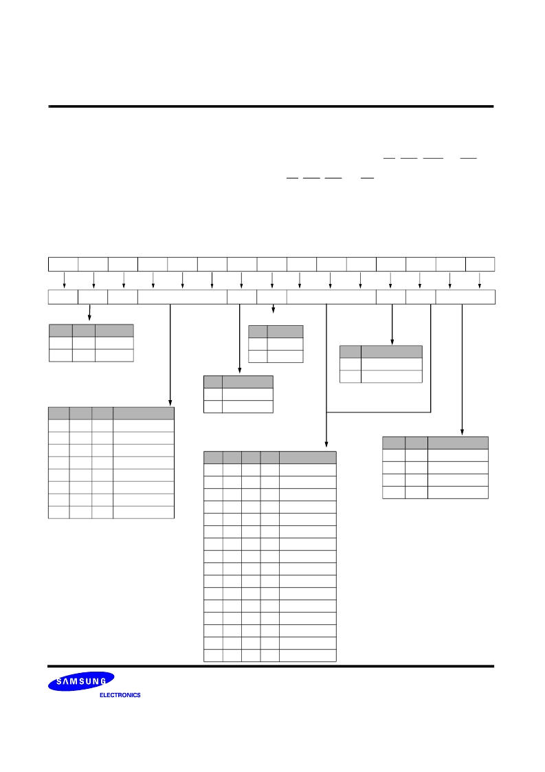
The mode register stores the data for controlling the various operating modes of GDDR3 SDRAM. It programs CAS
latency, addressing mode, test mode and various vendor specific options to make GDDR3 SDRAM useful for variety of dif-
ferent applications. The default value of the mode register is not defined, therefore the mode register must be written after
EMRS setting for the proper operation. The mode register is written by asserting low on CS, RAS, CAS and WE (The
GDDR3 SDRAM should be in active mode with CKE already high prior to writing into the mode register). The state of
address pins A
0
~ A
11
and BA
0
, BA
1
,
BA
2
in the same cycle as CS, RAS, CAS and WE going low is written in the mode
register. Minimum clock cycles specified as tMRD are required to complete the write operation in the mode register. The
mode register contents can be changed using the same command and clock cycle requirements during operation as long
as all banks are in the idle state. The mode register is divided into various fields depending on functionality. The Burst
length uses A
0
~ A
1
. CAS latency (read latency from column address) uses A
2
, A
6
~ A
4
. A
7
is used for test mode. A
8
is
used for DLL reset. A
9
~ A
11
are used for Write latency. Refer to the table for specific codes for various addressing modes
and CAS latencies.
MODE REGISTER SET(MRS)
CAS Latency
A
2
0
0
0
0
0
0
0
0
1
1
1
1
1
1
1
1
A
6
0
0
0
0
1
1
1
1
0
0
0
0
1
1
1
1
A
5
0
0
1
1
0
0
1
1
0
0
1
1
0
0
1
1
A
4
0
1
0
1
0
1
0
1
0
1
0
1
0
1
0
1
CAS Latency
8
9
10
11
4
5
6
7
Reserved(12)
Reserved(13)
Reserved(14)
Reserved(15)
Reserved
Reserved
Reserved
Reserved
BA
2
BA
1
BA
0
A
11
A
10
A
9
A
8
A
7
A
6
A
5
A
4
A
3
A
2
A
1
A
0
Test Mode
A
7
0
1
mode
Normal
Test
Burst Type
A
3
0
1
Burst Type
Sequential
Reserved
DLL
A
8
0
1
DLL Reset
No
Yes
RFU
0
0
WL
DLL
TM
CAS Latency
BT
CL
Burst Length
Burst Length
A
1
0
0
1
1
A
0
0
1
0
1
Burst Length
Reserved
Reserved
4
8
BA
1
0
0
BA
0
0
1
A
n
~ A
0
MRS
EMRS
Write Latency
A
11
0
0
0
0
1
1
1
1
A
10
0
0
1
1
0
0
1
1
A
9
0
1
0
1
0
1
0
1
Write Latency
Reserved
1
2
3
4
5
6
7
Note : DLL reset is self-clearing
RFU(Reserved for future use)
should stay "0" during MRS cycle
相關(guān)PDF資料 |
PDF描述 |
|---|---|
| K4J52324QC-BJ12 | 512Mbit GDDR3 SDRAM |
| K4J52324QC-BJ14 | 512Mbit GDDR3 SDRAM |
| K4M281633F | 2M x 16Bit x 4 Banks Mobile SDRAM in 54FBGA |
| K4M281633F-C | 2M x 16Bit x 4 Banks Mobile SDRAM in 54FBGA |
| K4M281633F-F1L | 2M x 16Bit x 4 Banks Mobile SDRAM in 54FBGA |
相關(guān)代理商/技術(shù)參數(shù) |
參數(shù)描述 |
|---|---|
| K4J52324QC-BJ12 | 制造商:SAMSUNG 制造商全稱(chēng):Samsung semiconductor 功能描述:512Mbit GDDR3 SDRAM |
| K4J52324QC-BJ14 | 制造商:SAMSUNG 制造商全稱(chēng):Samsung semiconductor 功能描述:512Mbit GDDR3 SDRAM |
| K4J52324QE-BC12000 | 制造商:Samsung Semiconductor 功能描述: |
| K4J52324QE-BC14000 | 制造商:Samsung Semiconductor 功能描述: |
| K4J52324QE-BC16000 | 制造商:Samsung Semiconductor 功能描述:GDDR3 SDRAM X32 BOC - Trays |
發(fā)布緊急采購(gòu),3分鐘左右您將得到回復(fù)。