- 您現(xiàn)在的位置:買賣IC網(wǎng) > PDF目錄374275 > K4J52324QC-BC16 (SAMSUNG SEMICONDUCTOR CO. LTD.) 512Mbit GDDR3 SDRAM PDF資料下載
參數(shù)資料
| 型號(hào): | K4J52324QC-BC16 |
| 廠商: | SAMSUNG SEMICONDUCTOR CO. LTD. |
| 英文描述: | 512Mbit GDDR3 SDRAM |
| 中文描述: | 512MB的GDDR3 SDRAM的 |
| 文件頁數(shù): | 47/57頁 |
| 文件大小: | 1246K |
| 代理商: | K4J52324QC-BC16 |
第1頁第2頁第3頁第4頁第5頁第6頁第7頁第8頁第9頁第10頁第11頁第12頁第13頁第14頁第15頁第16頁第17頁第18頁第19頁第20頁第21頁第22頁第23頁第24頁第25頁第26頁第27頁第28頁第29頁第30頁第31頁第32頁第33頁第34頁第35頁第36頁第37頁第38頁第39頁第40頁第41頁第42頁第43頁第44頁第45頁第46頁當(dāng)前第47頁第48頁第49頁第50頁第51頁第52頁第53頁第54頁第55頁第56頁第57頁
- 47 -
Rev 1.0 (Mar 2005)
512M GDDR3 SDRAM
K4J52324QC-B
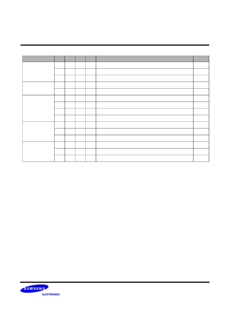
TRUTH TABLE - CURRENT STATE BANK
n
- COMMAND TO BANK
n
NOTES :
1. This table applies when CKE
n-1
was HIGH and CKE
n
is HIGH (see CKE Truth Table) and after t
XSNR
has been met
(if the previous state was self refresh).
2. This table is bank-specific, except where noted (i.e., the current state is for a specific bank and the commands shown
are those allowed to be issued to that bank when in that state). Exceptions are covered in the notes below.
3. Current state definitions :
Idle : The bank has been precharged, and t
RP
has been met.
Row Active : A row in the bank has been activated, and t
RCD
has been met.
No data bursts/accesses and no register accesses are in progress.
Read : A READ burst has been initiated, with auto precharge disabled.
Write : A WRITE burst has been initiated, with auto precharge disabled.
4. The following states must not be interrupted by a command issued to the same bank. COMMAND INHIBIT or NOP
commands, or allowable commands to the other bank should be issued on any clock edge occurring during these
states. Allowable commands to the other bank are determined by its current state and truth table- current state bank
n
command to bank
n
. and according to truth table - current state bank
n
-command to bank
m.
Precharging : Starts with registration of a PRECHARGE command and ends when t
RP
is met.
Once t
RP
is met, the bank will be in the idle state.
Row Activating : Starts with registration of an ACTIVE command and ends when t
RCD
is met.
Once t
RCD
is met, the bank will be in the :row active" state.
CURRENT STATE
/CS
/RAS
/CAS
/WE
COMMAND/ ACTION
NOTES
Any
H
X
X
X
DESELECT (NOP/ continue previous operation)
L
H
H
H
NO OPERATION (NOP/continue previous operation)
X
H
L
H
DATA TERMINATOR DISABLE
Idle
L
L
H
H
ACTIVE (Select and activate row)
L
L
L
H
AUTO REFRESH
7
Row Active
L
L
L
L
LOAD MODE REGISTER
7
L
H
L
H
READ (Select column and start READ burst)
10
L
H
L
L
WRITE (Select Column and start WRITE burst)
10
L
L
H
L
PRECHARGE (Deactivate row in bank or banks)
8
Read
(Auto-Precharge
Disable)
L
H
L
H
READ (Select column and start new READ burst)
10
L
H
L
L
WRITE (Select column and start WRITE burst)
10, 12
L
L
H
L
PRECHARGE (Only after the READ burst is complete)
8
Write
(Auto-Precharge
Disabled)
L
H
L
H
READ (Select column and start READ burst)
10, 11
L
H
L
L
WRITE (Select column and start new WRITE burst)
10
L
L
H
L
PRECHARGE (Only after the WRITE burst is complete)
8, 11
相關(guān)PDF資料 |
PDF描述 |
|---|---|
| K4J52324QC-BC20 | 512Mbit GDDR3 SDRAM |
| K4J52324QC-BJ12 | 512Mbit GDDR3 SDRAM |
| K4J52324QC-BJ14 | 512Mbit GDDR3 SDRAM |
| K4M281633F | 2M x 16Bit x 4 Banks Mobile SDRAM in 54FBGA |
| K4M281633F-C | 2M x 16Bit x 4 Banks Mobile SDRAM in 54FBGA |
相關(guān)代理商/技術(shù)參數(shù) |
參數(shù)描述 |
|---|---|
| K4J52324QC-BC20 | 制造商:SAMSUNG 制造商全稱:Samsung semiconductor 功能描述:512Mbit GDDR3 SDRAM |
| K4J52324QC-BJ12 | 制造商:SAMSUNG 制造商全稱:Samsung semiconductor 功能描述:512Mbit GDDR3 SDRAM |
| K4J52324QC-BJ14 | 制造商:SAMSUNG 制造商全稱:Samsung semiconductor 功能描述:512Mbit GDDR3 SDRAM |
| K4J52324QE-BC12000 | 制造商:Samsung Semiconductor 功能描述: |
| K4J52324QE-BC14000 | 制造商:Samsung Semiconductor 功能描述: |
發(fā)布緊急采購,3分鐘左右您將得到回復(fù)。