- 您現在的位置:買賣IC網 > PDF目錄374255 > K4D263238E-GC33 (SAMSUNG SEMICONDUCTOR CO. LTD.) DIODE ZENER SINGLE 300mW 16.1Vz 10mA-Izt 0.02547 0.05uA-Ir 12 SOT-23 3K/REEL PDF資料下載
參數資料
| 型號: | K4D263238E-GC33 |
| 廠商: | SAMSUNG SEMICONDUCTOR CO. LTD. |
| 英文描述: | DIODE ZENER SINGLE 300mW 16.1Vz 10mA-Izt 0.02547 0.05uA-Ir 12 SOT-23 3K/REEL |
| 中文描述: | 100萬x 32Bit的× 4銀行圖形雙數據速率同步DRAM的雙向數據選通和DLL |
| 文件頁數: | 13/17頁 |
| 文件大小: | 310K |
| 代理商: | K4D263238E-GC33 |
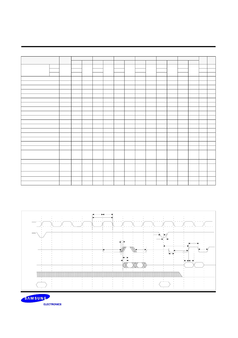
128M GDDR SDRAM
K4D263238E-GC
- 13 -
Rev 1.7 (Nov. 2003)
AC CHARACTERISTICS
*1.
The cycle to cycle jitter over 1~6 cycle short term jitter.
Parameter
Symbol
-25
-2A
-33
-36
-40
-45
Unit Note
Min
-
-
2.5
0.45
Max
Min
-
2.86
-
0.45
Max
Min
-
3.3
Max
Min
-
3.6
Max
Min
-
4.0
Max
Min
4.5
-
Max
CK cycle time
CL=3
CL=4
CL=5
t
CK
4
4
10
10
10
10
ns
ns
ns
tCK
tCK
ns
ns
ns
tCK
tCK
tCK
ns
tCK
tCK
tCK
tCK
ns
ns
ns
ns
CK high level width
t
CH
t
CL
t
DQSCK
t
AC
t
DQSQ
t
RPRE
t
RPST
t
DQSS
t
WPRES
t
WPREH
t
WPST
t
DQSH
t
DQSL
0.55
0.55
0.45
0.55
0.45
0.55
0.45
0.55
0.45
0.55
CK low level width
0.45
0.55
0.45
0.55
0.45
0.55
0.45
0.55
0.45
0.55
0.45
0.55
DQS out access time from CK
-0.55
0.55
-0.55
0.55
-0.55
0.55
-0.6
0.6
-0.6
0.6
-0.7
0.7
Output access time from CK
-0.55
0.55
-0.55
0.55
-0.55
0.55
-0.6
0.6
-0.6
-0.6
-0.7
0.7
Data strobe edge to Dout edge
-
0.35
-
0.35
-
0.35
-
0.40
-
0.40
-
0.45
1
Read preamble
0.9
1.1
0.9
1.1
0.9
1.1
0.9
1.1
0.9
1.1
0.9
1.1
Read postamble
0.4
0.6
0.4
0.6
0.4
0.6
0.4
0.6
0.4
0.6
0.4
0.6
CK to valid DQS-in
0.85
1.15
0.85
1.15
0.85
1.15
0.85
1.15
0.8
1.2
0.8
1.2
DQS-In setup time
0
-
0
-
0
-
0
-
0.
-
0.
-
DQS-in hold time
0.35
-
0.35
-
0.35
-
0.35
-
0.35
-
0.3
-
DQS write postamble
0.4
0.6
0.4
0.6
0.4
0.6
0.4
0.6
0.4
0.6
0.4
0.6
DQS-In high level width
0.45
0.55
0.45
0.55
0.45
0.55
0.45
0.55
0.45
0.55
0.45
0.55
DQS-In low level width
Address and Control input setup
t
IS
Address and Control input hold
0.45
0.55
0.45
0.55
0.45
0.55
0.45
0.55
0.45
0.55
0.45
0.55
0.8
-
0.8
-
0.8
-
0.9
-
0.9
-
1.0
-
t
IH
t
DS
t
DH
0.8
-
0.8
-
0.8
-
0.9
-
0.9
-
1.0
-
DQ and DM setup time to DQS
0.35
-
0.35
-
0.35
-
0.40
-
0.40
-
0.45
-
DQ and DM hold time to DQS
0.35
tCLmin
or
tCHmin
-
tHP-
t
QHS
-
0.35
tCLmin
or
tCHmin
-
tHP-
t
QHS
-
0.35
tCLmin
or
tCHmin
-
tHP-
t
QHS
-
0.40
tCLmin
or
tCHmin
-
tHP-
t
QHS
-
0.40
tCLmin
or
tCHmin
-
tHP-
t
QHS
-
0.45
tCLmin
or
tCHmin
-
tHP-
t
QHS
-
Clock half period
t
HP
-
-
-
-
-
-
ns
1
Data Hold skew factor
t
QHS
0.4
0.4
0.4
0.45
0.45
0.5
ns
Data output hold time from DQS
t
QH
-
-
-
-
-
-
ns
1
Jitter over 1~6 clock cycle error
t
J
*
1
t
DCERR
t
R
, t
F
-
75
-
75
-
85
-
95
-
100
-
105
ps
ps
ps
Cycle to cyde duty cycle error
-
75
-
75
-
85
-
95
-
100
-
105
Rise and fall times of CK
-
600
-
600
-
700
-
700
-
700
-
700
1
3
4
6
7
tCL
tCK
CK, CK
DQS
DQ
CS
DM
2
5
tIS
tIH
8
tDS tDH
0
tRPST
tRPRE
Db0
Db1
tDQSS
tDQSH
tDQSL
tCH
Qa1
Qa2
COMMAND
READA
WRITEB
tDQSQ
t
WPRES
t
WPREH
tDQSCK
tAC
Simplified Timing @ BL=2, CL=4
相關PDF資料 |
PDF描述 |
|---|---|
| K4D263238E-GC36 | DIODE ZENER TRIPLE ISOLATED 200mW 16.1Vz 10mA-Izt 0.02547 0.05uA-Ir 12 SOT-363 3K/REEL |
| K4D263238E-GC40 | DIODE ZENER SINGLE 300mW 17.9Vz 10mA-Izt 0.02545 0.05uA-Ir 14 SOT-23 3K/REEL |
| K4D263238E-GC45 | DIODE ZENER TRIPLE ISOLATED 200mW 17.88Vz 10mA-Izt 0.02545 0.05uA-Ir 14 SOT-363 3K/REEL |
| K4D263238G-GC | 128Mbit GDDR SDRAM |
| K4D263238G-GC2A | 128Mbit GDDR SDRAM |
相關代理商/技術參數 |
參數描述 |
|---|---|
| K4D263238E-GC36 | 制造商:SAMSUNG 制造商全稱:Samsung semiconductor 功能描述:1M x 32Bit x 4 Banks Graphic Double Data Rate Synchronous DRAM with Bi-directional Data Strobe and DLL |
| K4D263238E-GC40 | 制造商:SAMSUNG 制造商全稱:Samsung semiconductor 功能描述:1M x 32Bit x 4 Banks Graphic Double Data Rate Synchronous DRAM with Bi-directional Data Strobe and DLL |
| K4D263238E-GC45 | 制造商:SAMSUNG 制造商全稱:Samsung semiconductor 功能描述:1M x 32Bit x 4 Banks Graphic Double Data Rate Synchronous DRAM with Bi-directional Data Strobe and DLL |
| K4D263238F | 制造商:SAMSUNG 制造商全稱:Samsung semiconductor 功能描述:1M x 32Bit x 4 Banks Double Data Rate Synchronous DRAM with Bi-directional Data Strobe and DLL |
| K4D263238F-QC40 | 制造商:SAMSUNG 制造商全稱:Samsung semiconductor 功能描述:1M x 32Bit x 4 Banks Double Data Rate Synchronous DRAM with Bi-directional Data Strobe and DLL |
發(fā)布緊急采購,3分鐘左右您將得到回復。