- 您現(xiàn)在的位置:買賣IC網(wǎng) > PDF目錄362814 > ISO100CP Optically-Coupled Linear ISOLATION AMPLIFIER PDF資料下載
參數(shù)資料
| 型號: | ISO100CP |
| 元件分類: | 隔離放大器 |
| 英文描述: | Optically-Coupled Linear ISOLATION AMPLIFIER |
| 中文描述: | 光耦合線性隔離放大器 |
| 文件頁數(shù): | 7/15頁 |
| 文件大小: | 202K |
| 代理商: | ISO100CP |
ISO100
7
THEORY OF OPERATION
The ISO100 is fundamentally a unity gain current amplifier
intended to transfer small signals between electrical circuits
separated by high voltages or different references. In most
applications, an output voltage is obtained by passing the
output current through the feedback resistor (R
F
).
The ISO100 uses a single light emitting diode (LED) and a
pair of photodiode detectors coupled together to isolate the
output signal from the input.
Figure 1 shows a simplified diagram of the amplifier. I
REF1
and I
REF2
are required only for bipolar operation to generate
a midscale reference. The LED and photodiodes (D
1
and D
2
)
are arranged such that the same amount of light falls on each
photodiode. Thus, the currents generated by the diodes
match very closely. As a result, the transfer function de-
pends upon optical match rather than absolute performance.
Laser-trimming of the components improves matching and
enhances accuracy, while negative feedback improves lin-
earity. Negative feedback around A
1
occurs through the
optical path formed by the LED and D
1
. The signal is
transferred across the isolation barrier by the matched light
path to D
2
.
The overall isolation amplifier is noninverting (a positive
going input produces a positive going output).
INSTALLATION AND
OPERATING INSTRUCTIONS
UNIPOLAR OPERATION
In Figure 1, assume a current, I
IN
, flows out of the ISO100
(I
IN
must be negative in unipolar operation). This causes the
voltage at pin 15 to decrease. Because the amplifier is
inverting, the output of A
1
increases, driving current through
the LED. As the LED light output increases, D
1
responds by
generating an increasing current. The current increases until
the sum of the currents in and out of the input node (–Input
to A
1
) is zero. At that point, the negative feedback through
D
1
has stabilized the loop, and the current I
D1
equals the
input current plus the bias current. As a result, no bias
current flows in the source. Since D
1
and D
2
are matched
(I
D1
= I
D2
), I
IN
is replicated at the output via D
2
. Thus, A
1
functions as a unity-gain current amplifier, and A
2
is a
current-to-voltage converter, as described below.
Current produced by D
2
must either flow into A
2
or R
F
.
Since A
2
is designed for low bias current (
≈
10nA), almost all
of the current flows through R
F
to the output. The output
voltage then becomes:
V
O
= (I
D2
)R
F
= (I
D1
±
I
OS
)R
F
≈
–(–I
IN
)R
F
= I
IN
R
F
where, I
OS
is the difference between A
1
and A
2
bias currents.
For input voltage operation I
IN
can be replaced by a voltage
source (V
IN
) and series resistor (R
IN
), since the summing
node of the op amp is essentially at ground. Thus, I
IN
=
V
IN
/R
IN
.
Unipolar operation does have some constraints, however. In
this mode the input current must be negative so as to produce
a positive output voltage from A
1
to turn the LED on. A
current more negative than 20nA is necessary to keep the
LED turned on and the loop stabilized. When this condition
is not met, the output may be indeterminant. Many sensors
generate unidirectional signals, e.g., photoconductive and
photodiode devices, as well as some applications of thermo-
couples. However, other applications do require bipolar
operation of the ISO100.
(1)
BIPOLAR OPERATION
To activate the bipolar mode, reference currents as shown in
Figure 1 are attached to the input nodes of the op amps. The
input stage stabilizes just as it did in unipolar operation.
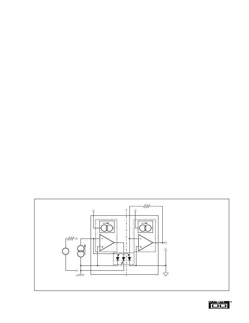
FIGURE 1. Simplified Block Diagram of the ISO100.
A
1
16
15
18
D
1
D
2
A
2
8
Isolation
Barrier
7
3
I
REF2
R
F
I
REF1
Input Common
Output Common
17
Optical
Assembly
LED
V
OUT
=
I
IN
R
F
V
OUT
R
IN
–In
I
IN
V
IN
–
+In
Input Circuit
Output Circuit
Connect pins 15 and 16 for bipolar,
and pins 16 and 17 for unipolar.
Connect pins 7 and 8 for bipolar,
and pins 8 and 9 for unipolar.
9
+
相關(guān)PDF資料 |
PDF描述 |
|---|---|
| ISO113 | Low-Cost, High-Voltage, Internally Powered OUTPUT ISOLATION AMPLIFIER |
| ISO113B | Low-Cost, High-Voltage, Internally Powered OUTPUT ISOLATION AMPLIFIER |
| ISO122 | Precision Lowest Cost ISOLATION AMPLIFIER |
| ISO122JP | Precision Lowest Cost ISOLATION AMPLIFIER |
| ISO122JU | Precision Lowest Cost ISOLATION AMPLIFIER |
相關(guān)代理商/技術(shù)參數(shù) |
參數(shù)描述 |
|---|---|
| ISO102 | 功能描述:隔離放大器 Wide BW Std Hermetic Sig Iso Buffer Amp RoHS:否 制造商:Texas Instruments 輸入補(bǔ)償電壓:1.5 mV 共模抑制比(最小值):95 dB 帶寬:60 KHz 工作電源電壓:3.3 V 電源電流:8 mA 工作溫度范圍:- 40 C to + 105 C 安裝風(fēng)格:SMD/SMT 封裝 / 箱體:SOP-8 封裝:Tube |
| ISO102/ISO106 | 制造商:BB 制造商全稱:BB 功能描述:ISO102. ISO106 - SIGNAL ISOLATION BUFFER AMPLIFIERS |
| ISO102B | 功能描述:隔離放大器 Wide BW Std Herm Sig Iso Buffer Amp RoHS:否 制造商:Texas Instruments 輸入補(bǔ)償電壓:1.5 mV 共模抑制比(最小值):95 dB 帶寬:60 KHz 工作電源電壓:3.3 V 電源電流:8 mA 工作溫度范圍:- 40 C to + 105 C 安裝風(fēng)格:SMD/SMT 封裝 / 箱體:SOP-8 封裝:Tube |
| ISO103 | 功能描述:特殊用途放大器 Low-Cost Internally Pwrd Iso Amp RoHS:否 制造商:Texas Instruments 通道數(shù)量:Single 共模抑制比(最小值): 輸入補(bǔ)償電壓: 工作電源電壓:3 V to 5.5 V 電源電流:5 mA 最大功率耗散: 最大工作溫度:+ 70 C 最小工作溫度:- 40 C 安裝風(fēng)格:SMD/SMT 封裝 / 箱體:QFN-20 封裝:Reel |
| ISO103 | 制造商:Texas Instruments 功能描述:IC AMP ISOLATION DIP24 103 |
發(fā)布緊急采購,3分鐘左右您將得到回復(fù)。