- 您現(xiàn)在的位置:買賣IC網(wǎng) > PDF目錄362811 > ISC302C Optoelectronic PDF資料下載
參數(shù)資料
| 型號(hào): | ISC302C |
| 英文描述: | Optoelectronic |
| 中文描述: | 光電 |
| 文件頁數(shù): | 7/11頁 |
| 文件大小: | 141K |
| 代理商: | ISC302C |
ISC300
7
I
1
CKI
I
2
CKI
I
3
CKI
I
4
CKI
I
5
CKI
I
N
CKI
Optional Clock Driver
MEASUREMENT CHANNEL
CALIBRATION
The ISC300 is designed to allow easy system calibration
using its internal voltage reference. Programming pins A
0
,
A
1
and G allows offset and full scale errors in gains of 0.5
and 50 to be measured.
System calibration would typically proceed as follows:
Lab Calibration
Set ISC300 gain.
Set input to 0V reference, measure Offset.
Connect external precision V reference, measure Gain.
Remove external V reference and set input to 10V or
0.1V reference.
Offset and Gain are now calibrated to an external preci-
sion reference
—record the numbers.
Field Calibration
Set ISC300 gain.
Set input to 0V reference, measure Offset.
Set input to 10V or 0.1V, measure Gain.
Recalibrate system.
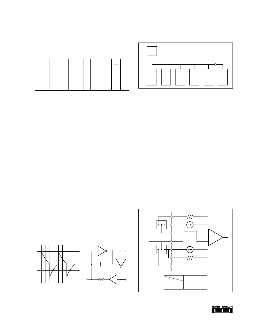
SYNCHRONIZATION
As the internal modulation frequencies of several ISC300s
can be marginally different, ‘beat’ frequencies ranging from
a few Hz to a few kHz can exist in multi ISC300 applica-
tions. The internal clock (see Figure 5) starts when power is
applied and runs at typically 50kHz. The ISC300 design
accommodates ‘internal synchronous’ noise which is caused
by minute timing differences, but synchronous beat fre-
quency noise will not be strongly attenuated, especially at
low frequencies if it is introduced via the power, signal or
ground paths. To overcome this problem, the design allows
the synchronization of each oscillator in the system to one
frequency. This is done by connecting the CKI (clock in)
39k
220pF
CKI
f = 50kHz
Simplified Schematic
FIGURE 5. CKI Input.
pins of each ISC300 in the system together (see Figure 6).
The ISC300 can also be synchronized by an external clock
driver.
INPUT
SELECT
GAIN
SELECT
SELECT
AND GAIN
A
1
A
0
G
RST
CLK
Com 1
0
0
0.5
0
No Change
1
0
+0.1V
0
1
50
1
No Change
1
1
+10V
1
0
Latch
1
^
Signal
1
1
RESET
0
X
FIGURE 7. Mode Selection Jumpers.
FIGURE 6. Synchronizing Multi-ISC300 Applications.
NOISE
Output noise is generated by the residual components of the
25kHz carrier that have not been removed from the signal.
This noise may be reduced by adding an output low pass
filter (see Figure 15 for an example of a 2 pole filter with
amplification, giving a
±
10V output). The filter time con-
stants should be set below the carrier frequency. The output
of the ISC300 is a switched capacitor and requires a high
impedance load to prevent degradation of linearity. Loads of
less than 1M
will cause an increase in noise at the carrier
frequency and will appear as ripple in the output waveform.
APPLICATIONS
This section describes the design criteria of various applica-
tions of the ISC300.
2, 3 AND 4 WIRE RESISTANCE MEASUREMENTS
Two wire resistance measurements are prone to errors due to
lead resistances. The voltage error can be significant since
the voltmeter measures on the lines supplying the RTD
+V
ISO
Sense 2
–In
+In
Filter and
MUX
Com 1
–In
+In
–V
ISO
I
REF2
–V
ISO
I
REF1
–V
ISO
Sense 1
Com 1
Com
3
1
2
J
1
1
J
2
2
3
Voltage
RTD
J
1
1-2
2-3
J
2
1-2
2-3
Mode
Jumper
PGA
20M
20M
相關(guān)PDF資料 |
PDF描述 |
|---|---|
| ISC302D | Optoelectronic |
| ISC302E | Optoelectronic |
| ISC302F | Optoelectronic |
| ISC363 | Optoelectronic |
| ISC363A | Optoelectronic |
相關(guān)代理商/技術(shù)參數(shù) |
參數(shù)描述 |
|---|---|
| ISC302D | 制造商:未知廠家 制造商全稱:未知廠家 功能描述:Optoelectronic |
| ISC302E | 制造商:未知廠家 制造商全稱:未知廠家 功能描述:Optoelectronic |
| ISC302F | 制造商:未知廠家 制造商全稱:未知廠家 功能描述:Optoelectronic |
| ISC3242AS1 | 制造商:ISAHAYA 制造商全稱:Isahaya Electronics Corporation 功能描述:FOR LOW FREQUENCY POWOR AMPLIFY APPLICATION SILICON NPN EPITAXIAL TYPE |
| ISC3244AS1 | 制造商:ISAHAYA 制造商全稱:Isahaya Electronics Corporation 功能描述:FOR LOW FREQUENCY POWOR AMPLIFY APPLICATION SILICON NPN EPITAXIAL TYPE |
發(fā)布緊急采購,3分鐘左右您將得到回復(fù)。