- 您現(xiàn)在的位置:買賣IC網(wǎng) > PDF目錄351653 > 1-480304-0 (Tyco Electronics) .200" Centerline, 250 V, 13 A max. PDF資料下載
參數(shù)資料
| 型號: | 1-480304-0 |
| 廠商: | Tyco Electronics |
| 元件分類: | 終端 |
| 英文描述: | .200" Centerline, 250 V, 13 A max. |
| 中文描述: | .200" 間距, 250 V, 13 A 最大值 |
| 文件頁數(shù): | 33/98頁 |
| 文件大?。?/td> | 2948K |
| 代理商: | 1-480304-0 |
第1頁第2頁第3頁第4頁第5頁第6頁第7頁第8頁第9頁第10頁第11頁第12頁第13頁第14頁第15頁第16頁第17頁第18頁第19頁第20頁第21頁第22頁第23頁第24頁第25頁第26頁第27頁第28頁第29頁第30頁第31頁第32頁當(dāng)前第33頁第34頁第35頁第36頁第37頁第38頁第39頁第40頁第41頁第42頁第43頁第44頁第45頁第46頁第47頁第48頁第49頁第50頁第51頁第52頁第53頁第54頁第55頁第56頁第57頁第58頁第59頁第60頁第61頁第62頁第63頁第64頁第65頁第66頁第67頁第68頁第69頁第70頁第71頁第72頁第73頁第74頁第75頁第76頁第77頁第78頁第79頁第80頁第81頁第82頁第83頁第84頁第85頁第86頁第87頁第88頁第89頁第90頁第91頁第92頁第93頁第94頁第95頁第96頁第97頁第98頁
173
Catalog 82181
Dimensions are in inches and
Dimensions are shown for
USA: 1-800-522-6752
South America: 55-11-2103-6000
Revised 4-08
millimeters unless otherwise
reference purposes only.
Canada: 1-905-470-4425
Hong Kong: 852-2735-1628
specified. Values in brackets
Specifications subject
Mexico: 01-800-733-8926
Japan: 81-44-844-8013
www.tycoelectronics.com
are metric equivalents.
to change.
C. America: 52-55-1106-0803
UK: 44-8706-080-208
Universal MATE-N-LOK Connectors (Continued)
AMP
Soft Shell
Pin and Socket Connectors
Universal
MA
TE-N-LOK
Connectors
.250
[6.35]
Centerline
Standard
Density
Contacts
Split pin diameter .086 [2.18]
Stock thickness .012 [.305]
These contacts can be used in either
Universal MATE-N-LOK Plug or Cap
housings only.
Related Product Data
Product Specification
108-1031 Universal MATE-N-LOK
Connectors
Application Specification
114-1010 Universal MATE-N-LOK
Contacts
Performance Characteristics—
pages 169-170
Technical Documents— pages 169
and 205-206
Application Tooling— pages 207-210
Housings—page 174
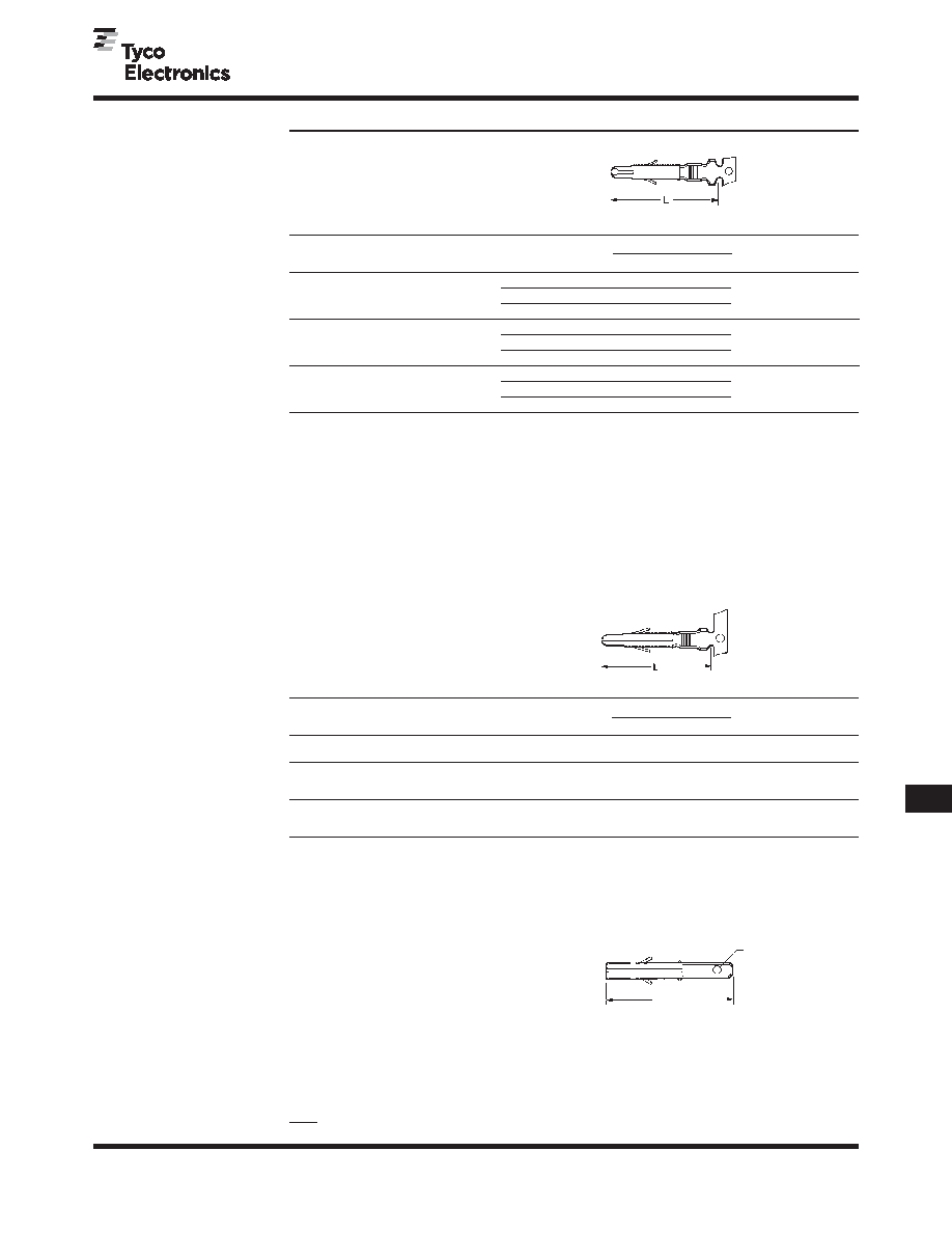
Split Pins
Wire Size Range
Ins. Dia.
L
Contact Part Number
HDM
Hand Tool
AWG [mm2]
Range
Dim.
Material & Finish
Applicator
Part No.
Strip Form
Loose Piece
Part No.
24-18
.040-.100
.790
Brass, Pre-tin
350699-1
350706-1
466320-13
[.2-.8]
1.02-2.54
20.06
Brass, Gold1
350699-2
350706-2
466320-23
91510-1
Brass, Select Gold2
350699-7
350706-7
466320-43
20-14
.060-.130
.790
Brass, Pre-tin
350687-1
350705-1
687763-13
[.5-2.0]
1.52-3.30
20.06
Brass, Gold1
350687-2
350705-2
687763-23
91500-1
Brass, Select Gold2
350687-7
350705-7
687763-63
.130-.200
.810
Brass, Pre-tin
350700-1
350707-1
687926-13
91508-14
3.30-5.08
20.57
Brass, Gold1
350700-2
350707-2
687926-23
91506-14
Brass, Select Gold2
350700-7
350707-7
687926-63
1
Gold Finish — Plated with .000030 [.000762] min. gold in mating area and inside wire barrel over .000050 [.00127]
min. nickel underplate on entire contact.
2
Select Gold Finish — Plated with .000030 [.000762] min. gold in mating area over .000050 [.00127] min. nickel
underplate on entire contact.
3
HDM Applicator part number ending in -1, is used on AMPOMATOR CLS Machine with T or G Terminators, -2 is
used on AMP-O-LECTRIC Model K Machine, -4 & -6 are used on AMP-O-LECTRIC Model G Machine. See
pages 207-210 for further information.
4
Hand Tool No. 91508-1 for wire size 20-18 AWG. Hand Tool No. 91506-1 for wire size 16-14 AWG.
Notes:
1. Split pins recommended for use in housings having 6, 9, 12 and 15 circuits to reduce mating force.
2. Phosphor bronze material contacts are available for use in high temperature/humidity cycling applications,
consult Tyco Electronics.
Note: This contact will accept a 110
Series FASTON Receptacle — Part
No. 350871-1 (strip form) allowing
simple field wiring or wiring changes.
Grounding Pins
(.100 [2.54] longer than standard pin)
(Mate first, break last, not for interrupting
current)
Wire Size Range
Ins. Dia.
L
Contact Part Number
HDM
Hand Tool
AWG [mm2]
Range
Dim.
Material & Finish
Applicator
Part No.
Strip Form
Loose Piece
Part No.
24-18
.060-.130
.890
Brass, Pre-tin
770210-1
—
567216-22
—
[.2-.8]
1.52-3.30
22.60
567216-32
20-14
.060-.130
.890
687763-12
Brass, Pre-tin
350654-1
350669-1
687763-22
91500-1
[.5-2.0]
1.52-3.30
22.60
687763-62
466597-12
12-10
.200 max.1
.910
Phos. Brz., Pre-tin
770234-3
—
466597-22
—
[3.0-5.0]
5.08
23.11
466597-32
1
There is no insulation barrel on this contact. Insulation maximum diameter is limited by the housing.
2
HDM Applicator part number ending in -1 is used on AMPOMATOR CLS Machine with T or G Terminators, -2 is
used on AMP-O-LECTRIC Model K Machine, -3 & -6 are used on AMP-O-LECTRIC Model G Machine. See pages
207-210 for further information.
Programmable Connector
Contact
(Socket with 110 Series Special
FASTON Tab)
Material and Finish
Brass, pre-tin
.805
[20.45]
.048
[1.22] Dia.
Part Number
350877-1
20-14
[.5-2.0]
or
2@18 [.8]
Note: All part numbers are RoHS Compliant.
相關(guān)PDF資料 |
PDF描述 |
|---|---|
| 1-480305-0 | .200" Centerline, 250 V, 13 A max. |
| 1-480305-2 | .200" Centerline, 250 V, 13 A max. |
| 1-480305-9 | .200" Centerline, 250 V, 13 A max. |
| 1-480318-0 | .200" Centerline, 250 V, 13 A max. |
| 1-480318-4 | .200" Centerline, 250 V, 13 A max. |
相關(guān)代理商/技術(shù)參數(shù) |
參數(shù)描述 |
|---|---|
| 1-480305 | 制造商:TE Connectivity 功能描述:.200" Centerline, 250 V, 13 A max. |
| 1-480305-0 | 功能描述:電源到板 PIN PANEL 3 CIRCUITS RoHS:否 制造商:TE Connectivity / AMP 系列:5787444 產(chǎn)品類型:Connectors 觸點類型: 電壓額定值:50 V 電流額定值: 節(jié)距: 位置/觸點數(shù)量:5 安裝風(fēng)格:Through Hole 端接類型: 觸點電鍍:Tin |
| 1-480305-2 | 功能描述:電源到板 03P CAP HSG F/H RED RoHS:否 制造商:TE Connectivity / AMP 系列:5787444 產(chǎn)品類型:Connectors 觸點類型: 電壓額定值:50 V 電流額定值: 節(jié)距: 位置/觸點數(shù)量:5 安裝風(fēng)格:Through Hole 端接類型: 觸點電鍍:Tin |
| 1-480305-9 | 功能描述:電源到板 03P CMNL CAP HSG F/H RoHS:否 制造商:TE Connectivity / AMP 系列:5787444 產(chǎn)品類型:Connectors 觸點類型: 電壓額定值:50 V 電流額定值: 節(jié)距: 位置/觸點數(shù)量:5 安裝風(fēng)格:Through Hole 端接類型: 觸點電鍍:Tin |
| 1-480306-1 | 功能描述:端子 .25 INSULATED FLAG RoHS:否 制造商:AVX 產(chǎn)品:Junction Box - Wire to Wire 系列:9826 線規(guī):26-18 接線柱/接頭大小: 絕緣: 顏色:Red 型式:Female 觸點電鍍:Tin over Nickel 觸點材料:Beryllium Copper, Phosphor Bronze 端接類型:Crimp |
發(fā)布緊急采購,3分鐘左右您將得到回復(fù)。