- 您現(xiàn)在的位置:買賣IC網 > PDF目錄362808 > IC43R16160-5TG 4M x 16 Bit x 4 Banks (256-MBIT) DDR SDRAM PDF資料下載
參數資料
| 型號: | IC43R16160-5TG |
| 英文描述: | 4M x 16 Bit x 4 Banks (256-MBIT) DDR SDRAM |
| 中文描述: | 4米× 16位× 4個銀行(256兆)DDR SDRAM內存 |
| 文件頁數: | 8/56頁 |
| 文件大?。?/td> | 1271K |
| 代理商: | IC43R16160-5TG |
第1頁第2頁第3頁第4頁第5頁第6頁第7頁當前第8頁第9頁第10頁第11頁第12頁第13頁第14頁第15頁第16頁第17頁第18頁第19頁第20頁第21頁第22頁第23頁第24頁第25頁第26頁第27頁第28頁第29頁第30頁第31頁第32頁第33頁第34頁第35頁第36頁第37頁第38頁第39頁第40頁第41頁第42頁第43頁第44頁第45頁第46頁第47頁第48頁第49頁第50頁第51頁第52頁第53頁第54頁第55頁第56頁
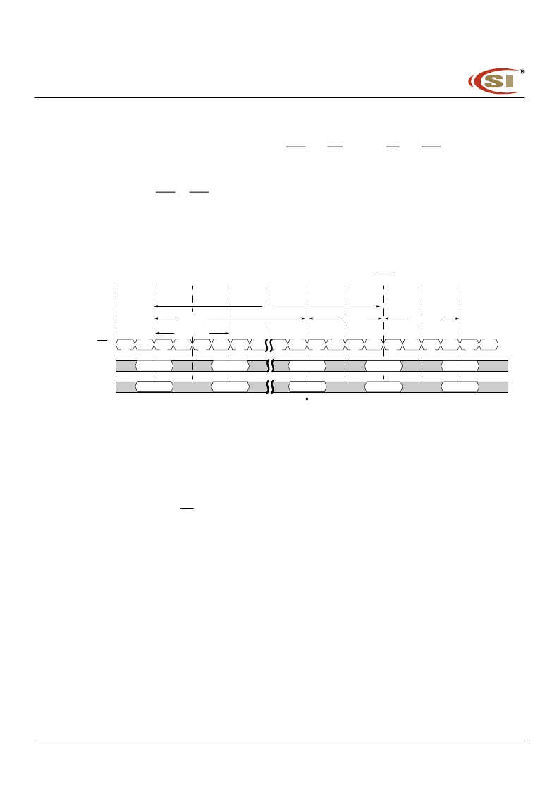
Bank Activate Command
The Bank Activate command is issued by holding CAS and WE high with CS and RAS low at the rising
edge of the clock. The DDR SDRAM has four independent banks, so two Bank Select addresses (BA
0
and
BA
1
) are supported. The Bank Activate command must be applied before any Read or Write operation can
be executed. The delay from the Bank Activate command to the first Read or Write command must meet or
exceed the minimum RAS to CAS delay time (t
RCD
min). Once a bank has been activated, it must be pre-
charged before another Bank Activate command can be applied to the same bank. The minimum time interval
between interleaved Bank Activate commands (Bank A to Bank B and vice versa) is the Bank to Bank delay
time (t
RRD
min).
Bank Activation Timing
Read Operation
With the DLL enabled, all devices operating at the same frequency within a system are ensured to have
the same timing relationship between DQ and DQS relative to the CK input regardless of device density, pro-
cess variation, or technology generation.
The data strobe signal (DQS) is driven off chip simultaneously with the output data (DQ) during each read
cycle. The same internal clock phase is used to drive both the output data and data strobe signal off chip to
minimize skew between data strobe and output data. This internal clock phase is nominally aligned to the
input differential clock (CK, CK) by the on-chip DLL. Therefore, when the DLL is enabled and the clock fre-
quency is within the specified range for proper DLL operation, the data strobe (DQS), output data (DQ), and
the system clock (CK) are all nominally aligned.
Since the data strobe and output data are tightly coupled in the system, the data strobe signal may be de-
layed and used to latch the output data into the receiving device. The tolerance for skew between DQS and
DQ (t
DQSQ
) is tighter than that possible for CK to DQ (t
AC
) or DQS to CK (t
DQSCK
).
T0
T1
T2
T3
Tn
Tn+1
Tn+2
Tn+3
Tn+4
Tn+5
(
CAS Latency = 2; Burst Length = Any)
t
RRD
(min)
t
RP
(min)
t
RC
t
RCD
(min)
Begin Precharge Bank A
CK,
CK
BA/Address
Command
Bank/Col
Read/A
Bank/Row
Activate/A
Activate/B
Pre/A
Bank/Row
Activate/A
Bank
Bank/Row
t
RAS
(min)
IC4
3R16160
8
Integrated Circuit Solution Inc.
DDR001
-
0B
1
1
/
10
/
2004
相關PDF資料 |
PDF描述 |
|---|---|
| IC43R16160-6T | 4M x 16 Bit x 4 Banks (256-MBIT) DDR SDRAM |
| IC43R16160-6TG | 4M x 16 Bit x 4 Banks (256-MBIT) DDR SDRAM |
| IC43R16160-7T | 4M x 16 Bit x 4 Banks (256-MBIT) DDR SDRAM |
| IC43R16160-7TG | 4M x 16 Bit x 4 Banks (256-MBIT) DDR SDRAM |
| ICS570 | Multiplier and Zero Delay Buffer |
相關代理商/技術參數 |
參數描述 |
|---|---|
| IC43R16160-6T | 制造商:ICSI 制造商全稱:Integrated Circuit Solution Inc 功能描述:4M x 16 Bit x 4 Banks (256-MBIT) DDR SDRAM |
| IC43R16160-6TG | 制造商:ICSI 制造商全稱:Integrated Circuit Solution Inc 功能描述:4M x 16 Bit x 4 Banks (256-MBIT) DDR SDRAM |
| IC43R16160-7T | 制造商:ICSI 制造商全稱:Integrated Circuit Solution Inc 功能描述:4M x 16 Bit x 4 Banks (256-MBIT) DDR SDRAM |
| IC43R16160-7TG | 制造商:ICSI 制造商全稱:Integrated Circuit Solution Inc 功能描述:4M x 16 Bit x 4 Banks (256-MBIT) DDR SDRAM |
| IC43R16160E-5TL | 制造商:Integrated Silicon Solution Inc 功能描述:256M, 2.5V, DDR, 16MX16, 200MHZ, 66 PIN |
發(fā)布緊急采購,3分鐘左右您將得到回復。