- 您現(xiàn)在的位置:買賣IC網(wǎng) > PDF目錄384469 > HY62VT08081E-DGI (Hynix Semiconductor Inc.) 32Kx8bit CMOS SRAM PDF資料下載
參數(shù)資料
| 型號: | HY62VT08081E-DGI |
| 廠商: | Hynix Semiconductor Inc. |
| 英文描述: | 32Kx8bit CMOS SRAM |
| 中文描述: | 32Kx8bit CMOS SRAM的 |
| 文件頁數(shù): | 9/12頁 |
| 文件大小: | 192K |
| 代理商: | HY62VT08081E-DGI |
HY62K(U,V)T08081E Series
Notes(WRITE CYCLE):
1. A write occurs during the overlap of a low /CS and a low /WE. A write begins at the latest transition
among /CS going low and /WE going low: A write ends at the earliest transition among /CS going high
and /WE going high. t
WP
is measured from the beginning of write to the end of write.
2. t
CW
is measured from the later of /CS going low to the end of write .
3. t
AS
is measured from the address valid to the beginning of write.
4. t
WR
is measured from the end of write to the address change. t
WR is
applied in case a write ends as /CS,
or /WE going high.
5. If /OE and /WE are in the read mode during this period, and the I/O pins are in the output low-Z state,
input of opposite phase of the output must not be applied because bus contention can occur.
6. If /CS goes low simultaneously with /WE going low, or after /WE going low, the outputs remain in high
impedance state.
7. D
OUT
is the same phase of the latest written data in this write cycle.
8. D
OUT
is the read data of the new address.
DATA RETENTION CHARACTERISTIC
Vcc = 2.7~3.6V, T
A
= 0
°
C to 70
°
C (Normal)/-25
°
C to 85
°
C (Extended) /-40
°
C to 85
°
C (Industrial),
unless otherwise specified.
Symbol
Parameter
Test Condition
V
DR
Vcc for Data Retention
CS>Vcc-0.2V,
V
IN
>Vcc-0.2V or V
IN
<Vss+0.2V
I
CCDR
Data Retention Current
Vcc=3.0V,
/CS>Vcc - 0.2V,
V
IN
>Vcc - 0.2V or
V
IN
<Vss + 0.2V
tCDR
Chip Deselect to Data
Retention Time
tR
Operating Recovery Time
Timing Diagram
Notes
1. Typical values are under the condition of T
A
= 25
°
C.
2. tRC is read cycle time.
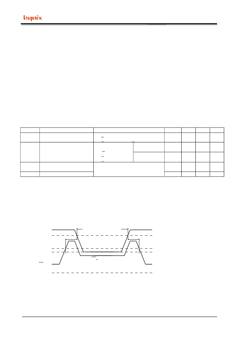
DATA RETENTION TIMING DIAGRAM
VCC
DATA RETENTION MODE
Rev 02 / Apr. 2001
8
Min
2.0
-
Typ
-
0.5
Max
3.6
5
Unit
V
uA
0~70
°
C
-25~85
°
C or
-40~85
°
C
-
0.5
8
uA
See Data Retention
0
-
-
ns
tRC
(2)
-
-
ns
CS
VDR
CS>VCC-0.2V
tCDR
tR
VSS
2.7V/3.0V
2.2V
相關(guān)PDF資料 |
PDF描述 |
|---|---|
| HY62VT08081E-DTC | 32Kx8bit CMOS SRAM |
| HY62VT08081E-DTE | 32Kx8bit CMOS SRAM |
| HY62VT08081E-DTI | 32Kx8bit CMOS SRAM |
| HY62UT08081E-DGC | 32Kx8bit CMOS SRAM |
| HY62UT08081E-DGE | QSW-REED,10MM,10W,SMD |
相關(guān)代理商/技術(shù)參數(shù) |
參數(shù)描述 |
|---|---|
| HY6300 | 制造商:未知廠家 制造商全稱:未知廠家 功能描述:Converter IC |
| HY6316100AJ-15 | 制造商:未知廠家 制造商全稱:未知廠家 功能描述:x16 SRAM |
| HY6316100AJ-17 | 制造商:未知廠家 制造商全稱:未知廠家 功能描述:x16 SRAM |
| HY6316100AJ-20 | 制造商:未知廠家 制造商全稱:未知廠家 功能描述:x16 SRAM |
| HY6316100AJ-25 | 制造商:未知廠家 制造商全稱:未知廠家 功能描述:x16 SRAM |
發(fā)布緊急采購,3分鐘左右您將得到回復(fù)。