- 您現(xiàn)在的位置:買賣IC網(wǎng) > PDF目錄384420 > HI5810KIJ (HARRIS SEMICONDUCTOR) CMOS 10 Microsecond, 12-Bit, Sampling A/D Converter with Internal Track and Hold PDF資料下載
參數(shù)資料
| 型號: | HI5810KIJ |
| 廠商: | HARRIS SEMICONDUCTOR |
| 元件分類: | ADC |
| 英文描述: | CMOS 10 Microsecond, 12-Bit, Sampling A/D Converter with Internal Track and Hold |
| 中文描述: | 12-BIT SUCCESSIVE APPROXIMATION ADC, PARALLEL ACCESS, CDIP24 |
| 文件頁數(shù): | 8/12頁 |
| 文件大小: | 423K |
| 代理商: | HI5810KIJ |
6-1784
Theory of Operation
The HI5810 is a CMOS 12-bit, Analog-to-Digital Converter
that uses capacitor charge balancing to successively
approximate the analog input. A binarily weighted capacitor
network forms the A/D heart of the device. See the block
diagram for the HI5810.
The capacitor network has a common node which is
connected to a comparator. The second terminal of each
capacitor is individually switchable to the input, V
REF
+ or
V
REF
-.
During the first three clock periods of a conversion cycle, the
switchable end of every capacitor is connected to the input
and the comparator is being auto balanced at the capacitor
common node.
During the fourth period, all capacitors are disconnected
from the input; the one representing the MSB (D11) is
connected to the V
REF
+ terminal; and the remaining
capacitors to V
REF
-. The capacitor common node, after the
charges balance out, will indicate whether the input was
above
1
/
2
of (V
REF
+ - V
REF
-). At the end of the fourth
period, the comparator output is stored and the MSB
capacitor is either left connected to V
REF
+ (if the comparator
was high) or returned to V
REF
-. This allows the next
comparison to be at either
3
/
4
or
1
/
4
of (V
REF
+ - V
REF
-).
At the end of periods 5 through 14, capacitors representing
D10 through D1 are tested, the result stored, and each
capacitor either left at V
REF
+ or at V
REF
-.
At the end of the 15th period, when the LSB (D0) capacitor is
tested, (D0) and all the previous results are shifted to the
output registers and drivers. The capacitors are reconnected
to the input, the comparator returns to the balance state, and
the data ready output goes active. The conversion cycle is
now complete.
Analog Input
The analog input pin is a predominately capacitive load that
changes between the track and hold periods of the
conversion cycle. During hold, clock period 4 through 15, the
input loading is leakage and stray capacitance, typically less
than 5
μ
A and 20pF.
At the start of input tracking, clock period 1, some charge is
dumped back to the input pin. The input source must have low
enough impedance to dissipate the current spike by the end of
the tracking period as shown in Figure 13. The amount of
charge is dependent on supply and input voltages. The
average current is also proportional to clock frequency.
TABLE 1. PIN DESCRIPTIONS
PIN NO.
NAME
DESCRIPTION
1
DRDY Output flag signifying new data is available.
Goes high at end of clock period 15. Goes low
when new conversion is started.
2
D0
Bit-0 (Least Significant Bit, LSB).
3
D1
Bit 1.
4
D2
Bit 2.
5
D3
Bit 3.
6
D4
Bit 4.
7
D5
Bit 5.
8
D6
Bit 6.
9
D7
Bit 7.
10
D8
Bit 8.
11
D9
Bit 9.
12
V
SS
Digital Ground, (0V).
13
D10
Bit 10.
14
D11
Bit 11 (Most Significant Bit, MSB)
15
OEM
Three-State Enable for D4-D11. Active low
input.
16
V
AA
-
Analog Ground, (0V).
17
V
AA
+
Analog Positive Supply. (+5V) (See text.)
18
V
IN
Analog Input.
19
V
REF
+ Reference Voltage Positive Input, sets 4095
code end of input range.
20
V
REF
-
Reference Voltage Negative Input, sets 0
code end of input range.
21
STRT
Start Conversion Input active low, recognized
after end of clock period 15.
22
CLK
CLK Input or Output. Conversion functions are
synchronized to positive going edge (see text).
23
OEL
Three-State Enable for D0 D3. Active low input.
24
V
DD
Digital Positive Supply (+5V).
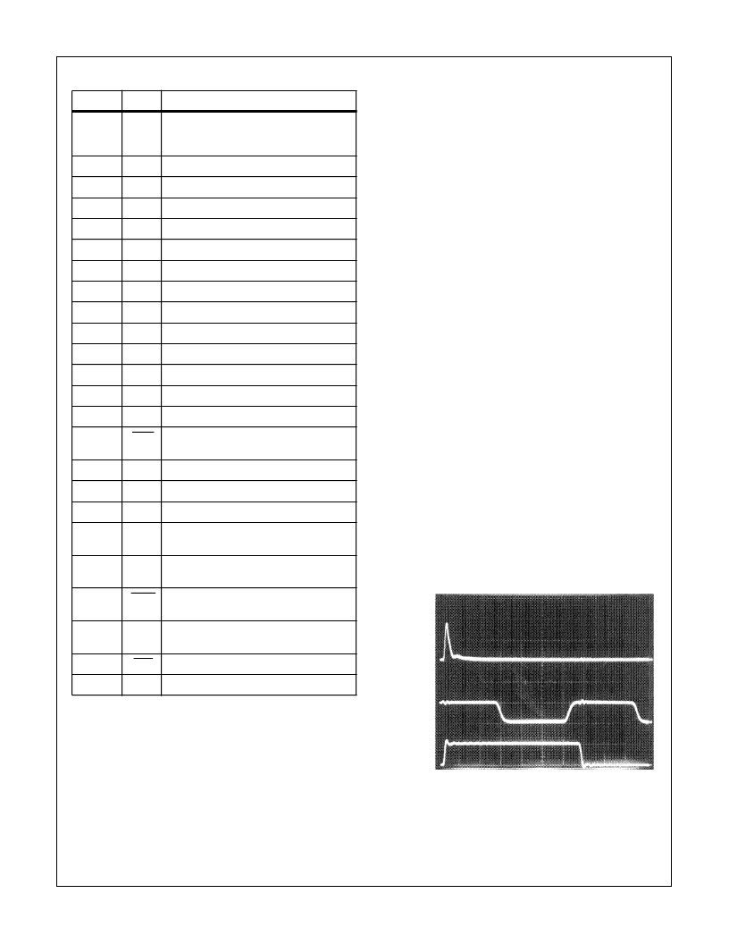
20mA
10mA
0mA
5V
0V
5V
0V
I
IN
CLK
DRDY
200ns/DIV.
CONDITIONS: V
DD
= V
AA
+ = 5.0V, V
REF
+ = 4.608V,
V
IN
= 4.608V, CLK = 750kHz, T
A
= 25
o
C
FIGURE 13. TYPICAL ANALOG INPUT CURRENT
HI5810
相關(guān)PDF資料 |
PDF描述 |
|---|---|
| HI5810KIP | CMOS 10 Microsecond, 12-Bit, Sampling A/D Converter with Internal Track and Hold |
| HI5812 | CMOS 20 Microsecond, 12-Bit, Sampling A/D Converter with Internal Track and Hold(CMOS 12位片內(nèi)帶跟蹤和保持電路的A/D轉(zhuǎn)換器) |
| HI5813 | CMOS 25Microsecond, 12-Bit, Sampling A/D Converter with Internal Track and Hold(CMOS 12位片內(nèi)帶跟蹤和保持電路的ADC) |
| HI5813JIB | CMOS 3.3V, 25 Microsecond, 12-Bit, Sampling A/D Converter with Internal Track and Hold |
| HI5813JIJ | CMOS 3.3V, 25 Microsecond, 12-Bit, Sampling A/D Converter with Internal Track and Hold |
相關(guān)代理商/技術(shù)參數(shù) |
參數(shù)描述 |
|---|---|
| HI5810KIP | 制造商:Rochester Electronics LLC 功能描述:- Bulk |
| HI5810KIPS2503 | 制造商:Rochester Electronics LLC 功能描述:- Bulk |
| HI5812 | 制造商:INTERSIL 制造商全稱:Intersil Corporation 功能描述:CMOS 20 Microsecond, 12-Bit, Sampling A/D Converter with Internal Track and Hold |
| HI5812_05 | 制造商:INTERSIL 制造商全稱:Intersil Corporation 功能描述:CMOS 20 Microsecond, 12-Bit, Sampling A/D Converter with Internal Track and Hold |
| HI5812JIB | 功能描述:ADC 12BIT 50KSPS 1.5LSB 24-SOIC RoHS:否 類別:集成電路 (IC) >> 數(shù)據(jù)采集 - 模數(shù)轉(zhuǎn)換器 系列:- 產(chǎn)品培訓(xùn)模塊:Lead (SnPb) Finish for COTS Obsolescence Mitigation Program 標(biāo)準(zhǔn)包裝:2,500 系列:- 位數(shù):12 采樣率(每秒):3M 數(shù)據(jù)接口:- 轉(zhuǎn)換器數(shù)目:- 功率耗散(最大):- 電壓電源:- 工作溫度:- 安裝類型:表面貼裝 封裝/外殼:SOT-23-6 供應(yīng)商設(shè)備封裝:SOT-23-6 包裝:帶卷 (TR) 輸入數(shù)目和類型:- |
發(fā)布緊急采購,3分鐘左右您將得到回復(fù)。