- 您現(xiàn)在的位置:買賣IC網(wǎng) > PDF目錄384407 > HGTP20N60B3 (FAIRCHILD SEMICONDUCTOR CORP) 72 MACROCELL 5 VOLT ISP CPLD - NOT RECOMMENDED for NEW DESIGN PDF資料下載
參數(shù)資料
| 型號: | HGTP20N60B3 |
| 廠商: | FAIRCHILD SEMICONDUCTOR CORP |
| 元件分類: | 功率晶體管 |
| 英文描述: | 72 MACROCELL 5 VOLT ISP CPLD - NOT RECOMMENDED for NEW DESIGN |
| 中文描述: | 40 A, 600 V, N-CHANNEL IGBT |
| 封裝: | TO-220AB ALTERNATE VERSION, 3 PIN |
| 文件頁數(shù): | 3/8頁 |
| 文件大小: | 140K |
| 代理商: | HGTP20N60B3 |
2001 Fairchild Semiconductor Corporation
HGTG20N60A4, HGTP20N60A4 Rev. B
Current Turn-On Delay Time
t
d(ON)I
t
rI
t
d(OFF)I
t
fI
E
ON1
E
ON2
E
OFF
R
θ
JC
IGBT and Diode at T
J
= 125
o
C
I
CE
= 20A
V
CE
= 390V
V
GE
= 15V
R
G
= 3
L = 500
μ
H
Test Circuit (Figure 20)
-
15
21
ns
Current Rise Time
-
13
18
ns
Current Turn-Off Delay Time
-
105
135
ns
Current Fall Time
-
55
73
ns
Turn-On Energy (Note 3)
-
115
-
μ
J
Turn-On Energy (Note 3)
-
510
600
μ
J
Turn-Off Energy (Note 2)
-
330
500
μ
J
Thermal Resistance Junction To Case
-
-
0.43
o
C/W
NOTES:
2. Turn-Off Energy Loss (E
OFF
) is defined as the integral of the instantaneous power loss starting at the trailing edge of the input pulse and ending
at the point where the collector current equals zero (I
CE
= 0A). All devices were tested per JEDEC Standard No. 24-1 Method for Measurement
of Power Device Turn-Off Switching Loss. This test method produces the true total Turn-Off Energy Loss.
3. Values for two Turn-On loss conditions are shown for the convenience of the circuit designer. E
ON1
is the turn-on loss of the IGBT only. E
ON2
is the turn-on loss when a typical diode is used in the test circuit and the diode is at the same T
J
as the IGBT. The diode type is specified in
Figure 20.
Electrical Specifications
T
J
= 25
o
C, Unless Otherwise Specified
(Continued)
PARAMETER
SYMBOL
TEST CONDITIONS
MIN
TYP
MAX
UNITS
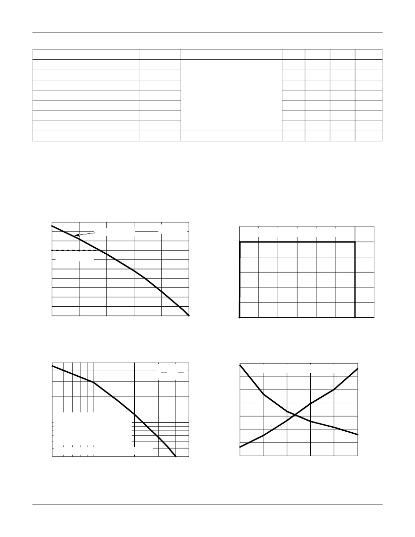
Typical Performance Curves
Unless Otherwise Specified
FIGURE 1. DC COLLECTOR CURRENT vs CASE
TEMPERATURE
FIGURE 2. MINIMUM SWITCHING SAFE OPERATING AREA
FIGURE 3. OPERATING FREQUENCY vs COLLECTOR TO
EMITTER CURRENT
FIGURE 4. SHORT CIRCUIT WITHSTAND TIME
T
C
, CASE TEMPERATURE (
o
C)
I
C
,
50
20
0
80
40
60
25
75
100
125
150
100
V
GE
= 15V
PACKAGE LIMIT
DIE CAPABILITY
V
CE
, COLLECTOR TO EMITTER VOLTAGE (V)
700
60
0
I
C
,
20
300
400
200
100
500
600
0
80
100
40
120
T
J
= 150
o
C, R
G
= 3
, V
GE
= 15V, L = 100
μ
H
f
M
,
5
I
CE
, COLLECTOR TO EMITTER CURRENT (A)
40
300
50
10
20
500
T
J
= 125
o
C, R
G
= 3
, L = 500
μ
H, V
CE
= 390V
100
40
30
f
MAX1
= 0.05 / (t
d(OFF)I
+ t
d(ON)I
)
f
MAX2
= (P
D
- P
C
) / (E
ON2
+ E
OFF
)
R
JC
= 0.43
o
C/W, SEE NOTES
P
C
= CONDUCTION DISSIPATION
(DUTY FACTOR = 50%)
T
C
75
o
C
V
GE
15V
V
GE
, GATE TO EMITTER VOLTAGE (V)
I
S
,
t
S
,
μ
s
10
11
12
15
0
2
10
100
250
350
450
14
13
14
4
6
8
12
150
200
300
400
V
CE
= 390V, R
G
= 3
, T
J
= 125
o
C
t
SC
I
SC
HGTG20N60A4, HGTP20N60A4
相關PDF資料 |
PDF描述 |
|---|---|
| HGTP20N60C3 | 45A, 600V, UFS Series N-Channel IGBT |
| HGTP2N120CND | 13A, 1200V, NPT Series N-Channel IGBTs(13A, 1200V,NPT系列N溝道絕緣柵雙極型晶體管) |
| HGTP5N120CN | 25A, 1200V, NPT Series N-Channel IGBT(25A, 1200V,NPT系列N溝道絕緣柵雙極型晶體管) |
| HGTP7N60B3D | 72 MACROCELL 3.3 VOLT ISP CPLD |
| HGTP7N60B3D | 3.3V 72-mc CPLD |
相關代理商/技術參數(shù) |
參數(shù)描述 |
|---|---|
| HGTP20N60B3R4035 | 制造商:Harris Corporation 功能描述: |
| HGTP20N60C3 | 制造商:INTERSIL 制造商全稱:Intersil Corporation 功能描述:45A, 600V, UFS Series N-Channel IGBT |
| HGTP20N60C3R | 制造商:Rochester Electronics LLC 功能描述:- Bulk 制造商:Harris Corporation 功能描述: |
| HGTP2N120BN | 制造商:INTERSIL 制造商全稱:Intersil Corporation 功能描述:12A, 1200V, NPT Series N-Channel IGBT |
| HGTP2N120BND | 制造商:INTERSIL 制造商全稱:Intersil Corporation 功能描述:12A, 1200V, NPT Series N-Channel IGBT with Anti-Parallel Hyperfast Diode |
發(fā)布緊急采購,3分鐘左右您將得到回復。