- 您現(xiàn)在的位置:買賣IC網(wǎng) > PDF目錄384407 > HGTP1N120CN (INTERSIL CORP) 6.2A, 1200V, NPT Series N-Channel IGBT(6.2A, 1200V, NPT系列N溝道絕緣柵雙極型晶體管) PDF資料下載
參數(shù)資料
| 型號(hào): | HGTP1N120CN |
| 廠商: | INTERSIL CORP |
| 元件分類: | 功率晶體管 |
| 英文描述: | 6.2A, 1200V, NPT Series N-Channel IGBT(6.2A, 1200V, NPT系列N溝道絕緣柵雙極型晶體管) |
| 中文描述: | 6.2 A, 1200 V, N-CHANNEL IGBT, TO-220AB |
| 文件頁數(shù): | 2/7頁 |
| 文件大?。?/td> | 77K |
| 代理商: | HGTP1N120CN |
2
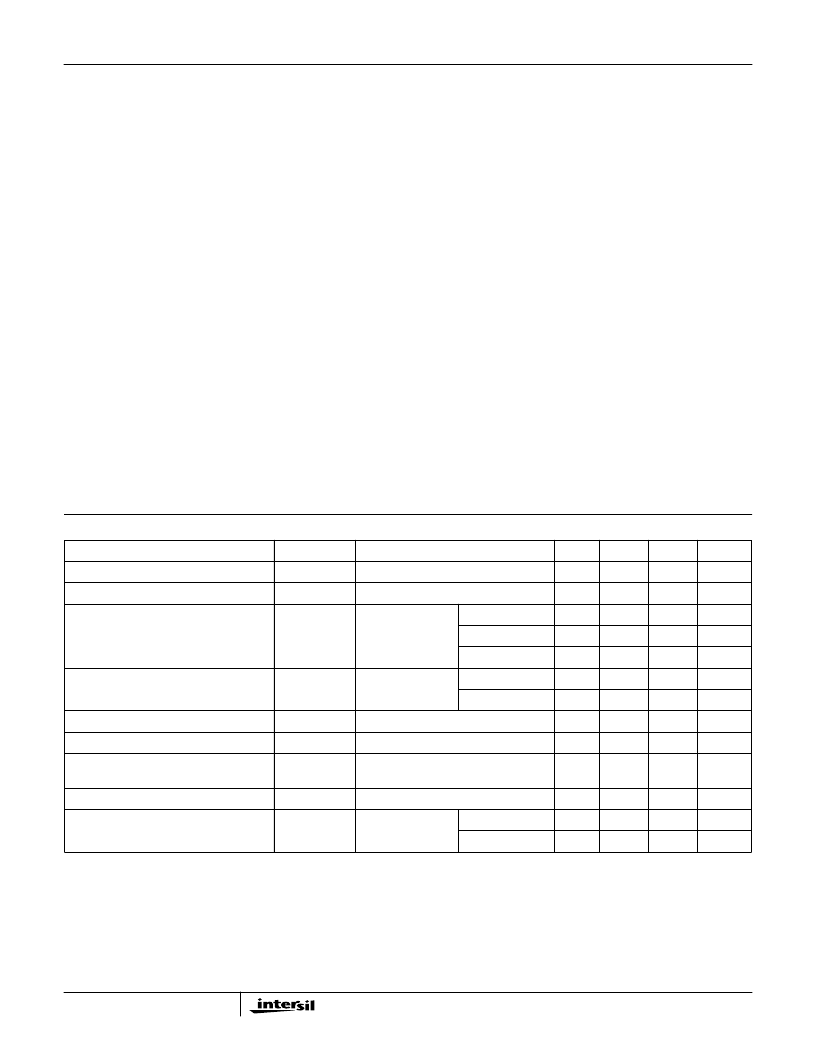
Absolute Maximum Ratings
T
C
= 25
o
C, Unless Otherwise Specified
HGTD1N120CNS,
HGTP1N120CN
1200
UNITS
V
Collector to Emitter Voltage . . . . . . . . . . . . . . . . . . . . . . . . . . . . . . . . . . . . . . . . . . . . . BV
CES
Collector Current Continuous
At T
C
= 25
o
C . . . . . . . . . . . . . . . . . . . . . . . . . . . . . . . . . . . . . . . . . . . . . . . . . . . . . . . . I
C25
At T
C
= 110
o
C . . . . . . . . . . . . . . . . . . . . . . . . . . . . . . . . . . . . . . . . . . . . . . . . . . . . . . I
C110
Collector Current Pulsed (Note 1) . . . . . . . . . . . . . . . . . . . . . . . . . . . . . . . . . . . . . . . . . . . I
CM
Gate to Emitter Voltage Continuous. . . . . . . . . . . . . . . . . . . . . . . . . . . . . . . . . . . . . . . . V
GES
Gate to Emitter Voltage Pulsed . . . . . . . . . . . . . . . . . . . . . . . . . . . . . . . . . . . . . . . . . . . V
GEM
Switching Safe Operating Area at T
J
= 150
o
C (Figure 2) . . . . . . . . . . . . . . . . . . . . . . . SSOA
Power Dissipation Total at T
C
= 25
o
C . . . . . . . . . . . . . . . . . . . . . . . . . . . . . . . . . . . . . . . . P
D
Power Dissipation Derating T
C
> 25
o
C . . . . . . . . . . . . . . . . . . . . . . . . . . . . . . . . . . . . . . . . . .
Forward Voltage Avalanche Energy (Note 2). . . . . . . . . . . . . . . . . . . . . . . . . . . . . . . . . . . E
AV
Operating and Storage Junction Temperature Range . . . . . . . . . . . . . . . . . . . . . . . . T
J
, T
STG
Maximum Lead Temperature for Soldering
Leads at 0.063in (1.6mm) from Case for 10s. . . . . . . . . . . . . . . . . . . . . . . . . . . . . . . . . . T
L
Package Body for 10s, see Tech Brief 334. . . . . . . . . . . . . . . . . . . . . . . . . . . . . . . . . . T
pkg
Short Circuit Withstand Time (Note 3) at V
GE
= 15V. . . . . . . . . . . . . . . . . . . . . . . . . . . . . t
SC
Short Circuit Withstand Time (Note 3) at V
GE
= 13V. . . . . . . . . . . . . . . . . . . . . . . . . . . . . t
SC
6.2
3.2
6
±
20
±
30
A
A
A
V
V
6A at 1200V
60
0.476
10
-55 to 150
W
W/
o
C
mJ
o
C
300
260
8
11
o
C
o
C
μ
s
μ
s
CAUTION: Stresses above those listed in “Absolute Maximum Ratings” may cause permanent damage to the device. This is a stress only rating and operation of the
device at these or any other conditions above those indicated in the operational sections of this specification is not implied.
NOTES:
1. Single Pulse; V
GE
= 15V; Pulse width limited by maximum junction temperature.
2. I
CE
= 7A, L = 400
μ
H, V
GE
= 15V, T
J
= 25
o
C.
3. V
CE(PK)
= 840V, T
J
= 125
o
C, R
G
= 82
.
Electrical Specifications
T
C
= 25
o
C, Unless Otherwise Specified
PARAMETER
SYMBOL
TEST CONDITIONS
MIN
TYP
MAX
UNITS
Collector to Emitter Breakdown Voltage
BV
CES
I
C
= 250
μ
A, V
GE
= 0V
1200
-
-
V
Emitter to Collector Breakdown Voltage
BV
ECS
I
C
= 10mA, V
GE
= 0V
15
-
-
V
Collector to Emitter Leakage Current
I
CES
V
CE
= BV
CES
T
C
= 25
o
C
T
C
= 125
o
C
T
C
= 150
o
C
T
C
= 25
o
C
T
C
= 150
o
C
-
-
250
μ
A
-
20
-
μ
A
-
-
1.0
mA
Collector to Emitter Saturation Voltage
V
CE(SAT)
I
C
= 1.0A,
V
GE
= 15V
-
2.05
2.4
V
-
2.75
3.2
V
Gate to Emitter Threshold Voltage
V
GE(TH)
I
C
= 50
μ
A, V
CE
= V
GE
6.0
7.1
-
V
Gate to Emitter Leakage Current
I
GES
V
GE
=
±
20V
T
J
= 150
o
C, R
G
= 82
,
V
GE
= 15V,
L = 2mH, V
CE(PK)
= 1200V
-
-
±
250
nA
Switching SOA
SSOA
6
-
-
A
Gate to Emitter Plateau Voltage
V
GEP
I
C
= 1.0A, V
CE
= 0.5 BV
CES
-
9.7
-
V
On-State Gate Charge
Q
G(ON)
I
C
= 1.0A,
V
CE
= 0.5 BV
CES
V
GE
= 15V
-
13
19
nC
V
GE
= 20V
-
16
28
nC
HGTD1N120CNS, HGTP1N120CN
相關(guān)PDF資料 |
PDF描述 |
|---|---|
| HGTP20N35G3VL | 20A, 350V N-Channel, Logic Level, Voltage Clamping IGBTs |
| HGTP20N35G3VL | 72 MACROCELL 5 VOLT ISP CPLD - NOT RECOMMENDED for NEW DESIGN |
| HGTP20N60A4 | 72 MACROCELL 5 VOLT ISP CPLD - NOT RECOMMENDED for NEW DESIGN |
| HGTP20N60A4 | 72 MACROCELL 5 VOLT ISP CPLD - NOT RECOMMENDED for NEW DESIGN |
| HGTP20N60B3 | 40A, 600V, UFS Series N-Channel IGBTs |
相關(guān)代理商/技術(shù)參數(shù) |
參數(shù)描述 |
|---|---|
| HGTP1N120CND | 制造商:INTERSIL 制造商全稱:Intersil Corporation 功能描述:6.2A, 1200V, NPT Series N-Channel IGBT with Anti-Parallel Hyperfast Diode |
| HGTP20N35F3ULR3935 | 制造商:Rochester Electronics LLC 功能描述:- Bulk |
| HGTP20N35F3VL | 制造商:Rochester Electronics LLC 功能描述:- Bulk 制造商:Harris Corporation 功能描述: |
| HGTP20N35G3VL | 功能描述:IGBT 晶體管 Coil Dri 20A 350V RoHS:否 制造商:Fairchild Semiconductor 配置: 集電極—發(fā)射極最大電壓 VCEO:650 V 集電極—射極飽和電壓:2.3 V 柵極/發(fā)射極最大電壓:20 V 在25 C的連續(xù)集電極電流:150 A 柵極—射極漏泄電流:400 nA 功率耗散:187 W 最大工作溫度: 封裝 / 箱體:TO-247 封裝:Tube |
| HGTP20N36G3VL | 制造商:FAIRCHILD 制造商全稱:Fairchild Semiconductor 功能描述:20A, 360V N-Channel, Logic Level, Voltage Clamping IGBTs |
發(fā)布緊急采購,3分鐘左右您將得到回復(fù)。