- 您現(xiàn)在的位置:買賣IC網(wǎng) > PDF目錄384398 > HE84770D (King Billion Electronics Co., Ltd.) 8-bit Micro-controller PDF資料下載
參數(shù)資料
| 型號: | HE84770D |
| 廠商: | King Billion Electronics Co., Ltd. |
| 英文描述: | 8-bit Micro-controller |
| 中文描述: | 8位微控制器 |
| 文件頁數(shù): | 23/29頁 |
| 文件大?。?/td> | 360K |
| 代理商: | HE84770D |
第1頁第2頁第3頁第4頁第5頁第6頁第7頁第8頁第9頁第10頁第11頁第12頁第13頁第14頁第15頁第16頁第17頁第18頁第19頁第20頁第21頁第22頁當(dāng)前第23頁第24頁第25頁第26頁第27頁第28頁第29頁
King Billion Electronics Co., Ltd
駿
億
電
子
股
份
有
限
公
司
HE84770D
HE80000 SERIES
program can operate normally. When abnormal conditions happen to cause the MCU to divert from
August 7, 2006
This specification is subject to change without notice. Please contact sales person for the latest version before use.
Page 23 of 29
V1.2
normal path, the WDT counter will not be cleared and reset signal will be generated.
WDT is the enabling signal generated by calculating 32768-clock overflow. Reset Register content is
same as TC1 (Timer1 clock), which uses the same clock count source. WDT function can be generated
in Normal, Slow and Idle Mode. However, WDT will not function during Sleep Mode (as the TC1
clock has stopped.)
15.
Digital-to-Analog Converter
The Digital-to-Analog converter (DAC) converts the 7-bit unsigned speech data written to PWMC to
proportional current output.
PWMC register
DA & PWM Data
Control
Bit 7
0
1
Bit 6
Bit 5
Bit 4
DA and PWM output value
-
Bit 3
Bit 2
Bit 1
Bit 0
PWM O/P driver
-
-
PWME
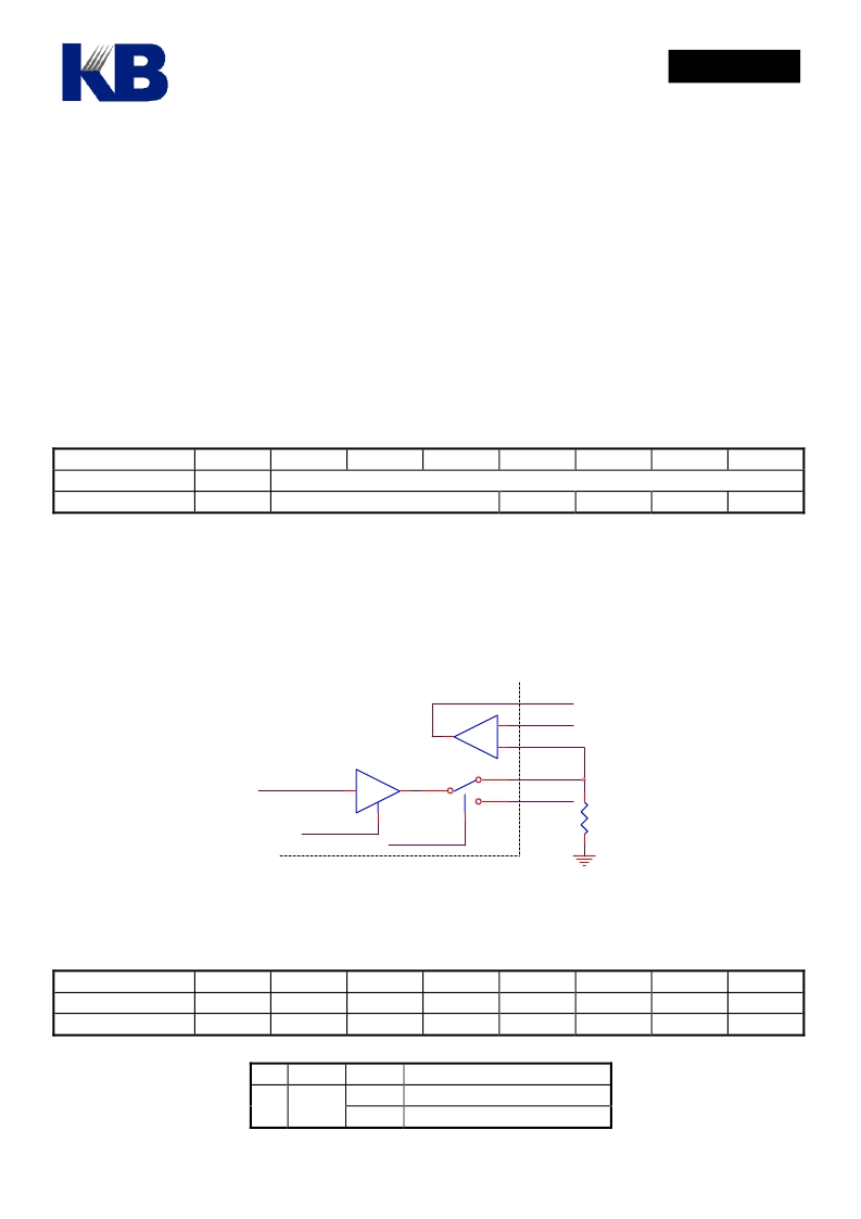
There are two output paths for the DAC. Either VO or DAO can be selected as output port of DAC by
VOC register when it is enabled. The VO output is primarily intended for speech generation, although it
is not necessary so, while the DAO output path can be used in conjunction with built-in OP comparator to
function as an Analog-to-Digital Converter as required in applications such as speech recording, speech
recognition or sensor interfaces.
OPO
OPIP
OPIN
DAO
PWMC[DATA]
VO
VOC[DAC]
VOC[OP]
R
DAC
+
-
1
0
OP
The DAC is enabled by DAC bit of VOC register. Please note that the DAC bit of VOC register will be
automatically cleared when the system enter Idle or Sleep mode. So it needs to be set again when
returning to Normal mode.
VOC register
Field
Reset
Bit 7
-
-
Bit 6
-
-
Bit 5
-
-
Bit 4
-
-
Bit 3
-
-
Bit 2
PWM
0
Bit 1
DAC
0
Bit 0
OP
0
Bit Name Value
Function description
DA Enable
DA Disable
1
0
1
DAC
相關(guān)PDF資料 |
PDF描述 |
|---|---|
| HE84770 | 8-bit Micro-controller |
| HE84G752B | 8-BIT MICRO-CONTROLLER |
| HE84G761B | 8-BIT MICRO-CONTROLLER |
| HE84G762B | 8-BIT MICRO-CONTROLLER |
| HE84G763B | 8-BIT MICRO-CONTROLLER |
相關(guān)代理商/技術(shù)參數(shù) |
參數(shù)描述 |
|---|---|
| HE84771(S) | 制造商:未知廠家 制造商全稱:未知廠家 功能描述: |
| HE847711(S) | 制造商:未知廠家 制造商全稱:未知廠家 功能描述: |
| HE84772(S) | 制造商:未知廠家 制造商全稱:未知廠家 功能描述: |
| HE847721(S) | 制造商:未知廠家 制造商全稱:未知廠家 功能描述: |
| HE84773(S) | 制造商:未知廠家 制造商全稱:未知廠家 功能描述: |
發(fā)布緊急采購,3分鐘左右您將得到回復(fù)。