- 您現(xiàn)在的位置:買賣IC網(wǎng) > PDF目錄384397 > HE83003 (King Billion Electronics Co., Ltd.) 8-BIT MICRO-CONTROLLER PDF資料下載
參數(shù)資料
| 型號: | HE83003 |
| 廠商: | King Billion Electronics Co., Ltd. |
| 英文描述: | 8-BIT MICRO-CONTROLLER |
| 中文描述: | 8位微控制器 |
| 文件頁數(shù): | 20/23頁 |
| 文件大?。?/td> | 226K |
| 代理商: | HE83003 |
King Billion Electronics Co., Ltd
駿
億
電
子
股
份
有
限
公
司
HE83003
HE80000 SERIES
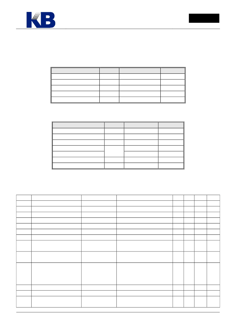
12.
Absolute Maximum Rating
September 8, 2004
This specification is subject to change without notice. Please contact sales person for the latest version before use.
20
V1.1
Item
Symbol
V
DD
V
IN
V
o
T
op
T
st
Rating
-0.5V ~ 7.0V
-0.5V ~ V
DD
+0.5V
-0.5V ~ V
DD
+0.5V
0
℃
~ 70
℃
-50
℃
~ 100
℃
Condition
Supply Voltage
Input Voltage
Output Voltage
Operating Temperature
Storage Temperature
13.
Recommended Operating Conditions
Item
Symbol
V
DD
V
IH
V
IL
Rating
2.4V ~ 5.56V
0.9 V
DD
~ V
DD
0.0V ~ 0.1 V
DD
8M Hz
4M Hz
0
0
C ~ 70
0
C
-50
0
C ~ 100
0
C
Condition
V
DD
=5.0V
V
DD
=2.4V
Supply Voltage
Input Voltage
Operating Frequency
Operating Temperature
Storage Temperature
Fmax.
T
op
T
st
14.
AC/DC Characteristics
Testing Condition: TEMP=25
℃
, VDD=3V±10%
PARAMETER
I
Fast
NORMAL Mode Current System
I
Slow
SLOW Mode Current
I
Idle
IDLE Mode Current
I
Sleep
Sleep Mode Current
I
oHPWM
PWM
Output Drive Current
PWMP, PWMN
*2
V
DD
=3V; V
OH
=2V
I
oLPWM
PWM
Output Sink Current
PWMP, PWMN
*2
V
DD
=3V; V
OL
=1V
I
oVO
DAC Output Current
VO
V
iH
Input High Voltage
I/O pins
CONDITION
2M ext. R/C
32.768K X’tal
32.769K X’tal
MIN TYP MAX UNIT
0.75
6
4
12
15
33
40
3
0.8
V
DD
1
9
7
1
mA
μA
μA
μA
mA
mA
mA
System
System
System
V
DD
=3V;VO=0~2V,Data=7F 2.5
V
V
iL
Input Low Voltage
I/O pins
0.2
V
DD
V
V
hys
Input Hysteresis Width
I/O, RSTP_N
Threshold=2/3V
DD
(input
from low to high)
Threshold=1/3V
DD
(input
from high to low)
V
OL
=2.0V
V
OL
=0.4V
V
IL
=GND, pull high
Internally
1/3
V
DD
V
I
OH
I
OL_1
I
IL_1
Output Drive Current
Output Sink Current
I/O pull-high
*1
I/O pull-low
*1
50
1.0
μA
mA
Input Low Current
RSTP_N
20
μA
相關(guān)PDF資料 |
PDF描述 |
|---|---|
| HE83005 | 8-BIT MICRO-CONTROLLER |
| HE83006 | 8-BIT MICRO-CONTROLLER |
| HE83015 | 8-BIT MICRO-CONTROLLER |
| HE83016 | 8-BIT MICRO-CONTROLLER |
| HE83115 | 8-BIT MICRO-CONTROLLER |
相關(guān)代理商/技術(shù)參數(shù) |
參數(shù)描述 |
|---|---|
| HE83005 | 制造商:KB 制造商全稱:KB 功能描述:8-BIT MICRO-CONTROLLER |
| HE83005(S) | 制造商:未知廠家 制造商全稱:未知廠家 功能描述: |
| HE83006 | 制造商:KB 制造商全稱:KB 功能描述:8-BIT MICRO-CONTROLLER |
| HE83006(S) | 制造商:未知廠家 制造商全稱:未知廠家 功能描述: |
| HE83007(S) | 制造商:未知廠家 制造商全稱:未知廠家 功能描述: |
發(fā)布緊急采購,3分鐘左右您將得到回復(fù)。