- 您現(xiàn)在的位置:買賣IC網(wǎng) > PDF目錄384393 > HC5517CB (HARRIS SEMICONDUCTOR) 3 REN Ringing SLIC For ISDN Modem/TA and WLL PDF資料下載
參數(shù)資料
| 型號(hào): | HC5517CB |
| 廠商: | HARRIS SEMICONDUCTOR |
| 元件分類: | 模擬傳輸電路 |
| 英文描述: | 3 REN Ringing SLIC For ISDN Modem/TA and WLL |
| 中文描述: | TELECOM-SLIC, PDSO28 |
| 文件頁數(shù): | 11/18頁 |
| 文件大小: | 175K |
| 代理商: | HC5517CB |
70
the SLIC. The signals are Battery Switch, F1 and Ring
Cadence (RC). The active application circuit and active
supervisory function are different for each mode, as shown
in the Table 2.
Mode Control Signals
The Battery Switch selects between the -80V and -24V
supplies. The Battery Switch circuitry is described in the
“Operation of the Battery Switch” section. A system alterna-
tive to the battery switch signal is to use a buffered version of
the SHD output to select the battery voltage. Another alter-
native is to control the output of a programmable battery
supply, removing the battery switch entirely from the applica-
tion circuit. F1 is used to put the SLIC in the power denial
mode. RC drives the base of T
2
, which is the transistor used
to control the centering voltage and MTU voltage. The three
control signals can be driven from a TTL logic source or an
open collector output
RINGING MODE
The ringing state, as the name indicates, is used to ring the
telephone with a -80V battery supply. The SLIC is designed
for balanced ringing with a differential gain of 40V/V across tip
and ring. Voltage feed amplifiers operating in the linear mode
are used to amplify the ringing signal. The linear amplifier
approach allows the system designer to define the shape and
amplitude of the ringing waveform. Both supervisory function
outputs, SHD and RTD, are active during ringing.
Spectral Content of the Ringing Signal
The shape of the waveform can range from sinusoidal to
trapezoidal. Sinusoidal waveforms are spectrally cleaner
than trapezoidal waveforms, although the latter does result
in lower power dissipation across the SLIC for a given RMS
amplitude. Systems where the ringing signal will be in prox-
imity to digital data lines will benefit from the sinusoidal ring-
ing capability of the HC5517. The slow edge rates of a
sinusoid will minimize coupling of the large amplitude ringing
signal. The linear amplifier architecture of the HC5517
allows the system designer to optimize the design for power
dissipation and spectral purity.
Amplitude of the Ringing Signal
Amplitude control is another benefit of the linear amplifier
architecture. Systems that require less ringing amplitude are
able to do so by driving the HC5517 with a lower level ringing
waveform. Solutions that use saturated amplifiers can only
vary the amplitude of the ringing signal by changing the
negative battery voltage to the SLIC.
HC5517 Through SLIC Ringing
The HC5517 is designed with a high gain input, V
RING
, that
the system drives while ringing the phone. V
RING
is one of
many signals summed at the inverting input to the tip feed
amplifier. The gain of the V
RING
signal through the tip feed
amplifier is set to 20V/V. The output of the tip feed amplifier
is summed at the inverting input of the ring feed amplifier,
configured for unity gain. The result is a differential gain of
40V/V across tip and ring of the ringing signal.
The ringing function requires an input ringing waveform and
a centering voltage. The ringing waveform is the signal from
the 4-wire side that is amplified by the SLIC to ring the tele-
phone. The centering voltage, as previously discussed, is a
positive DC offset that is applied to the V
RING
input along
with the ringing waveform. The HC5517 application circuit
provides the centering voltage, simplifying the system
interface to an AC coupled ringing waveform.
Ringer Equivalence Number
Before any further discussion, the Ringer Equivalence
Number or REN must be discussed. Based on FCC Part
68.313 a single REN can be defined as 5k
, 7k
or 8k
of
AC impedance at the ringing frequency. The ringing fre-
quency is based on the ringing types listed in Table 1 of the
FCC specification. The impedance of multiple REN is the
paralleling of a single REN. Therefore 5 REN can either be
1k
, 1.4k
or 1.6k
. The 7k
model of a single REN will be
used throughout the remainder of the data sheet.
Ringing Waveform
An amplitude of 1.2V
RMS
will deliver approximately 46V
RMS
to a 1 REN load, and 42V
RMS
to a 3 REN load. The ampli-
tude is REN dependent and is slightly attenuated by the
feedback scheme used for impedance matching. The ringing
waveform is cadenced, alternating between a 20Hz burst
and a silent portion between bursts. Bellcore specification
TR-NWT-000057 defines seven distinct ringing waveforms or
alerting (ringing) patterns. The following table lists each type.
Figure 8 shows the relationship of the cadenced ringing
waveform and the Battery Switch and RC control signals.
Also shown are the states of the MTU voltage and the
centering voltage.
The state of Battery Switch is indicated by the desired
battery voltage to the SLIC. The RC signal is used to enable
and disable the centering voltage and MTU voltage. RC
follows the ring signal in that it is high during the 20Hz burst
and low during the static part of the waveform.
Open Circuit Voltage During the Ringing Mode
The mutually exclusive relationship of the centering voltage
and MTU implies that both functions will not exist at the
same time. During the silent portion of the ringing waveform
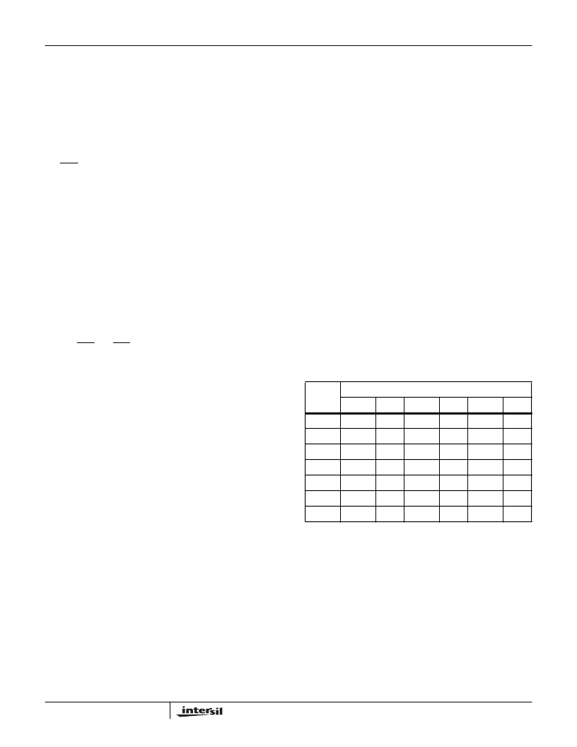
TABLE 1. DISTINCTIVE ALERTING PATTERNS
PATTERN
INTERVAL DURATION IN SECONDS
RINGING SILENT RINGING SILENT RINGING SILENT
A
0.4
0.2
0.4
0.2
0.8
4.0
B
0.2
0.1
0.2
0.1
0.6
4.0
C
0.8
0.4
0.8
0.4
D
0.4
0.2
0.6
4.0
E
1.2
4.0
F
1
±
0.2
3
±
0.3
G
0.3
0.2
1.0
0.2
0.3
4.0
HC5517
相關(guān)PDF資料 |
PDF描述 |
|---|---|
| HC5517CM | 3 REN Ringing SLIC For ISDN Modem/TA and WLL |
| HC5517IM | 3 REN Ringing SLIC For ISDN Modem/TA and WLL |
| HC5517IB | GIGATRUE 550 CAT PATCH CBL NO BOOT 6FT RD 25 PK |
| HC55180 | Extended Reach Ringing SLIC Family |
| HC55181 | Extended Reach Ringing SLIC Family |
相關(guān)代理商/技術(shù)參數(shù) |
參數(shù)描述 |
|---|---|
| HC5517CB96 | 制造商:Rochester Electronics LLC 功能描述:- Bulk |
| HC5517CM | 制造商:Harris Corporation 功能描述: |
| HC5517CM96 | 制造商:Rochester Electronics LLC 功能描述:- Bulk |
| HC5517IB | 制造商:Rochester Electronics LLC 功能描述:- Bulk |
| HC5517IM | 制造商:Rochester Electronics LLC 功能描述:- Bulk |
發(fā)布緊急采購,3分鐘左右您將得到回復(fù)。