- 您現(xiàn)在的位置:買賣IC網 > PDF目錄384393 > HC5517B (Intersil Corporation) Low Cost 3 REN Ringing SLIC for ISDN Modem/TA and WL PDF資料下載
參數(shù)資料
| 型號: | HC5517B |
| 廠商: | Intersil Corporation |
| 英文描述: | Low Cost 3 REN Ringing SLIC for ISDN Modem/TA and WL |
| 中文描述: | 低成本三任振鈴用戶接口的ISDN調制解調器/電訊和WL |
| 文件頁數(shù): | 9/11頁 |
| 文件大?。?/td> | 88K |
| 代理商: | HC5517B |
69
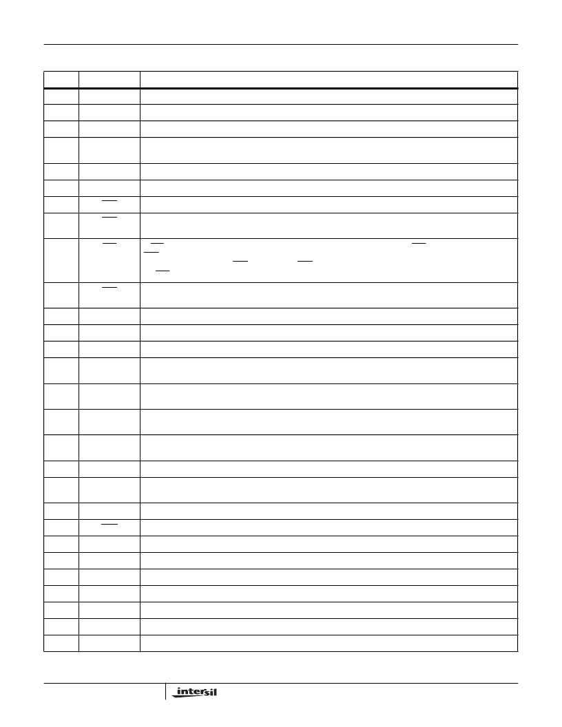
Pin Descriptions
PLCC
SYMBOL
DESCRIPTION
1
AGND
Analog Ground - Serves as a reference for the transmit output and receive input terminals.
2
V
CC
Positive Voltage Source - normally +5V DC.
3
V
REF
An external voltage connected to this pin will override the internal V
BAT
/2 reference.
4
F1
Power Denial - An active low TTL compatible logic control input. When enabled, the output of the ring amplifier will
ramp close to the output voltage of the tip amplifier.
5
F0
TTL compatible logic control input that controls multiplexing of the detector outputs.
6
RS
TTL compatible logic control input that must be tied high for proper SLIC operation.
7
SHD
Switch Hook Detection - An active low TTL compatible logic output. Indicates an off-hook condition.
8
RTD
Ring Trip Detection - An active low TTL compatible logic output. Indicates an off-hook condition when the phone is
ringing. May be used to indicate ring trip or ground key detection.
9
TST
A TTL logic input. A low on this pin will keep the SLIC in a power down mode. The TST pin, in conjunction with the
ALM pin, can provide thermal shutdown protection for the SLIC. Thermal shutdown is implemented by a system
controller that monitors the ALM pin. When the ALM pin is active (low), the system controller issues a command to
the TST pin (low) to power down the SLIC. The timing of the thermal recovery is controlled by the system controller.
10
ALM
A TTL compatible active low output which responds to the thermal detector circuit when a safe operating die
temperature has been exceeded.
11
I
LIMIT
Loop Current Limit - used with V
TX
to set the short loop current limiting conditions.
12
OUT1
The 4-wire output of the SLIC.
13
-IN1
The inverting input of the impedance matching amplifier. The non-inverting input is internally connected to AGND.
14
TIP SENSE
An analog input connected to the TIP (more positive) side of the subscriber loop through a feed resistor. Functions
with the RING terminal to receive voice signals and for loop monitoring purpose.
15
RING SENSE 1
An analog input connected to the RING (more negative) side of the subscriber loop through a feed resistor. Functions
with the TIP terminal to receive voice signals and for loop monitoring purposes.
16
RING SENSE 2
This is an internal sense mode that must be tied to RING SENSE 1 for proper SLIC operation. Also used during
unbalanced ringing.
17
V
RX
Receive Input, 4-Wire Side - A high impedance analog input. AC signals appearing at this input drive the Tip Feed
and Ring Feed amplifiers differentially.
18
NU
Not used in this application. This pin should be left floating.
19
V
TX
A low impedance analog voltage output which is proportional to the subscriber loop current. Since the DC level of
this output varies with loop current, capacitive coupling to IN1- is necessary.
20
RDI
TTL compatible input to drive the ring relay driver during unbalanced ringing.
21
RDO
Open collector relay driver used during unbalanced ringing.
22
BGND
Battery Ground - All loop current and some quiescent current flows from this terminal.
23
NU
Not used in this application. This pin should be either grounded or left floating.
24
V
RING
Low level ringing signal input.
25
TF
Output of the tip line feed amplifier.
26
RF
Output of the ring line feed amplifier.
27
V
BAT
The negative battery source, all loop current flows into this terminal.
28
RTI
Ring Trip Input - This pin is connected to the external negative peak detector output for ring trip detection.
HC5517B
相關PDF資料 |
PDF描述 |
|---|---|
| HC5517BCB | Low Cost 3 REN Ringing SLIC for ISDN Modem/TA and WL |
| HC5517BCM | Low Cost 3 REN Ringing SLIC for ISDN Modem/TA and WL |
| HC5517 | 3 REN Ringing SLIC For ISDN Modem/TA and WLL |
| HC5517CB | 3 REN Ringing SLIC For ISDN Modem/TA and WLL |
| HC5517CM | 3 REN Ringing SLIC For ISDN Modem/TA and WLL |
相關代理商/技術參數(shù) |
參數(shù)描述 |
|---|---|
| HC5517B WAF | 制造商:Harris Corporation 功能描述: |
| HC5517BCB | 制造商:Rochester Electronics LLC 功能描述:- Bulk 制造商:Harris Corporation 功能描述: |
| HC5517BCB96S2495 | 制造商:Rochester Electronics LLC 功能描述:- Bulk |
| HC5517BCM | 制造商:Rochester Electronics LLC 功能描述:- Bulk |
| HC5517CB | 制造商:Rochester Electronics LLC 功能描述:- Bulk |
發(fā)布緊急采購,3分鐘左右您將得到回復。