- 您現(xiàn)在的位置:買賣IC網(wǎng) > PDF目錄384393 > HC5515 (Intersil Corporation) ITU CO/PABX SLIC with Low Power Standby PDF資料下載
參數(shù)資料
| 型號: | HC5515 |
| 廠商: | Intersil Corporation |
| 英文描述: | ITU CO/PABX SLIC with Low Power Standby |
| 中文描述: | 國際電聯(lián)合作/交換機用戶接口低功耗待機 |
| 文件頁數(shù): | 15/17頁 |
| 文件大小: | 170K |
| 代理商: | HC5515 |
69
E
RX
= -10dBm, 1.0kHz signal, E
G
= 0, I
DCMET
= 23mA and is
computed using the following equation:
G
4-2
= 20
log (V
TR
/E
RX
) vary amplitude -40dBm to +3dBm,
or -55dBm to -40dBm and compare to -10dBm reading.
V
TR
and E
RX
are defined in Figure 9. The level is specified at
the 4-wire receive port and referenced to a 600
impedance
level.
23. Two-WireIdleChannelNoise -
The 2-wire idle channel noise
at V
TR
is specified with the 2-wire port terminated in 600
(R
L
)
and with the 4-wire receive port grounded (Reference Figure 10).
24. Four-WireIdleChannelNoise -
The 4-wire idle channel noise
at V
TX
is specified with the 2-wire port terminated in 600
(R
L
).
The noise specification is with respect to a 600
impedance
level at V
TX
. The 4-wire receive port is grounded (Reference
Figure 10).
25. HarmonicDistortion(2-Wireto4-Wire) -
The harmonic dis-
tortion is measured with the following conditions. E
G
= 0dBm
at 1kHz, I
DCMET
= 23mA. Measurement taken at V
TX
.
(Reference Figure 7).
26. HarmonicDistortion(4-Wireto2-Wire) -
The harmonic dis-
tortion is measured with the following conditions. E
RX
= 0dBm0.
Vary frequency between 300Hz and 3.4kHz, I
DCMET
= 23mA.
Measurement taken at V
TR
. (Reference Figure 9).
27. ConstantLoopCurrent -
The
calculated using the following equation:
constant
loop
current
is
I
L
= 2500 / (R
DC1
+ R
DC2
).
28. StandbyStateLoopCurrent -
The standby state loop current
is calculated using the following equation:
I
L
= [|V
BAT
| - 3] / [R
L
+1800], T
A
= 25
o
C.
29. PowerSupplyRejectionRatio -
Inject a 100mV
RMS
signal
(50Hz to 4kHz) on V
BAT
, V
CC
and V
EE
supplies. PSRR is
computed using the following equation:
PSRR = 20
log (V
TX
/V
IN
). V
TX
and V
IN
are defined in Figure 11.
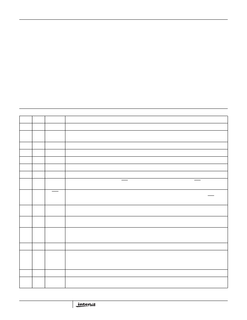
Pin Descriptions
PLCC
PDIP
SYMBOL
DESCRIPTION
1
RING
SENSE
Internally connected to output of RING power amplifier.
2
7
BGND
Battery Ground - To be connected to zero potential. All loop current and longitudinal current flow from this ground.
Internally separate from AGND but it is recommended that it is connected to the same potential as AGND.
4
8
V
CC
+5V power supply.
5
9
RINGRLY
Ring relay driver output.
6
10
V
BAT
Battery supply voltage, -24V to -56V.
7
11
R
SG
Saturation guard programming resistor pin.
8
12
NC
This pin is used during manufacturing.This pin is to be left open for proper SLIC operation .
9
13
E0
TTL compatible logic input. Enables the DET output when set to logic level zero and disables DET output when set to
a logic level one.
11
14
DET
Detector output. TTL compatible logic output. A zero logic level indicates that the selected detector was triggered (see
Truth Table for selection of Ground Key detector, Loop Current detector or the Ring Trip detector). The DET output is
an open collector with an internal pull-up of approximately 15k
to V
CC.
12
15
C2
TTLcompatiblelogicinput.ThelogicstatesofC1andC2determinetheoperatingstates(OpenCircuit,Active,Ringing
or Standby) of the SLIC.
13
16
C1
TTLcompatiblelogicinput.ThelogicstatesofC1andC2determinetheoperatingstates(OpenCircuit,Active,Ringing
or Standby) of the SLIC.
14
17
R
DC
DC feed current programming resistor pin. Constant current feed is programmed by resistors R
DC1
and R
DC2
connectedinseriesfromthispintothereceivesummingnode(RSN).TheresistorjunctionpointisdecoupledtoAGND
to isolate the AC signal components.
15
18
AGND
Analog ground.
16
19
RSN
Receive Summing Node. The AC and DC current flowing into this pin establishes the metallic loop current that flows
between tip and ring. The magnitude of the metallic loop current is 1000 times greater than the current into the RSN
pin. The constant current programming resistors and the networks for program receive gain and 2-wire impedance all
connect to this pin.
18
20
V
EE
-5V power supply.
19
21
V
TX
Transmit audio output. This output is equivalent to the TIP to RING metallic voltage. The network for programming the
2-wire input impedance connects between this pin and RSN.
HC5515
相關PDF資料 |
PDF描述 |
|---|---|
| HC5515CM | ITU CO/PABX SLIC with Low Power Standby |
| HC5515CP | ITU CO/PABX SLIC with Low Power Standby |
| HC5515IM | ITU CO/PABX SLIC with Low Power Standby |
| HC5515IP | ITU CO/PABX SLIC with Low Power Standby |
| HC5517B | Low Cost 3 REN Ringing SLIC for ISDN Modem/TA and WL |
相關代理商/技術參數(shù) |
參數(shù)描述 |
|---|---|
| HC5515_06 | 制造商:INTERSIL 制造商全稱:Intersil Corporation 功能描述:ITU CO/PABX SLIC with Low Power Standby |
| HC55150 | 制造商:INTERSIL 制造商全稱:Intersil Corporation 功能描述:Low Power Universal SLIC Family |
| HC55150CB | 制造商:Rochester Electronics LLC 功能描述:LOW PWR SLIC,POL REV/METERING,55DB BALANCE - Bulk |
| HC55150CBZ | 功能描述:電信線路管理 IC LW PWR SLIC POLV/MTRING 55DB RoHS:否 制造商:STMicroelectronics 產(chǎn)品:PHY 接口類型:UART 電源電壓-最大:18 V 電源電壓-最小:8 V 電源電流:30 mA 最大工作溫度:+ 85 C 最小工作溫度:- 40 C 安裝風格:SMD/SMT 封裝 / 箱體:VFQFPN-48 封裝:Tray |
| HC55150CM | 制造商:Rochester Electronics LLC 功能描述:LOW PWR SLIC,POL REV/METERING,55DB BALANCE - Bulk |
發(fā)布緊急采購,3分鐘左右您將得到回復。