- 您現(xiàn)在的位置:買賣IC網(wǎng) > PDF目錄384392 > HC-5509B (Intersil Corporation) ITU CO/Loop Carrier SLIC(ITU 環(huán)路載波芯片) PDF資料下載
參數(shù)資料
| 型號: | HC-5509B |
| 廠商: | Intersil Corporation |
| 英文描述: | ITU CO/Loop Carrier SLIC(ITU 環(huán)路載波芯片) |
| 中文描述: | 國際電聯(lián)合作/環(huán)路載波用戶接口(國際電聯(lián)環(huán)路載波芯片) |
| 文件頁數(shù): | 2/8頁 |
| 文件大小: | 89K |
| 代理商: | HC-5509B |
4-2
Absolute Maximum Ratings
(Note 1)
Thermal Information
Relay Drivers . . . . . . . . . . . . . . . . . . . . . . . . . . . . . . . . .-0.5V to 15V
Maximum Supply Voltages
(V
B+
) . . . . . . . . . . . . . . . . . . . . . . . . . . . . . . . . . . . . . .-0.5V to 7V
(V
B+
)-(V
B-
) . . . . . . . . . . . . . . . . . . . . . . . . . . . . . . . . . . . . . . . .75V
Operating Conditions
Operating Temperature Range
HC-5509B-5 . . . . . . . . . . . . . . . . . . . . . . . . . . . . . . . .0
o
C to 75
o
C
Relay Drivers . . . . . . . . . . . . . . . . . . . . . . . . . . . . . . . . . . .5V to 12V
Positive Power Supply (V
B+
) . . . . . . . . . . . . . . . . . . . . . . . . 5V
±
5%
Negative Power Supply (V
B-
). . . . . . . . . . . . . . . . . . . . .-42V to -58V
Loop Resistance (R
L
) . . . . . . . . . . . . . . . . 200
to 1750
(Note 2)
Thermal Resistance (Typical, Note 3)
SOIC Package . . . . . . . . . . . . . . . . . . .
Maximum Junction Temperature Plastic . . . . . . . . . . . . . . . . .150
o
C
Storage Temperature Range . . . . . . . . . . . . . . . . . . -65
o
C to 150
o
C
Maximum Lead Temperature (Soldering 10s) . . . . . . . . . . . . .300
o
C
(For SMD; SOIC - Lead Tips Only)
θ
JA
(
o
C/W)
72
θ
JC
(
o
C/W)
N/A
Die Characteristics
Transistor Count. . . . . . . . . . . . . . . . . . . . . . . . . . . . . . . . . . . . . .224
Diode Count. . . . . . . . . . . . . . . . . . . . . . . . . . . . . . . . . . . . . . . . . .28
Die Dimensions . . . . . . . . . . . . . . . . . . . . . . . . . . . . . . . . . 174 x 120
Substrate Potential. . . . . . . . . . . . . . . . . . . . . . . . . . . . . . Connected
Process . . . . . . . . . . . . . . . . . . . . . . . . . . . . . . . . . . . . . . .Bipolar-DI
CAUTION: Stresses above those listed in “Absolute Maximum Ratings” may cause permanent damage to the device. This is a stress only rating and operation of the
device at these or any other conditions above those indicated in the operational sections of this specification is not implied.
NOTES:
1. Absolute maximum ratings are limiting values, applied individually, beyond which the serviceability of the circuit may be impaired. Functional
operability under any of these conditions is not necessarily implied.
2. May Be Extended to 1900
With Application Circuit.
3.
θ
JA
is measured with the component mounted on an evaluation PC board in free air.
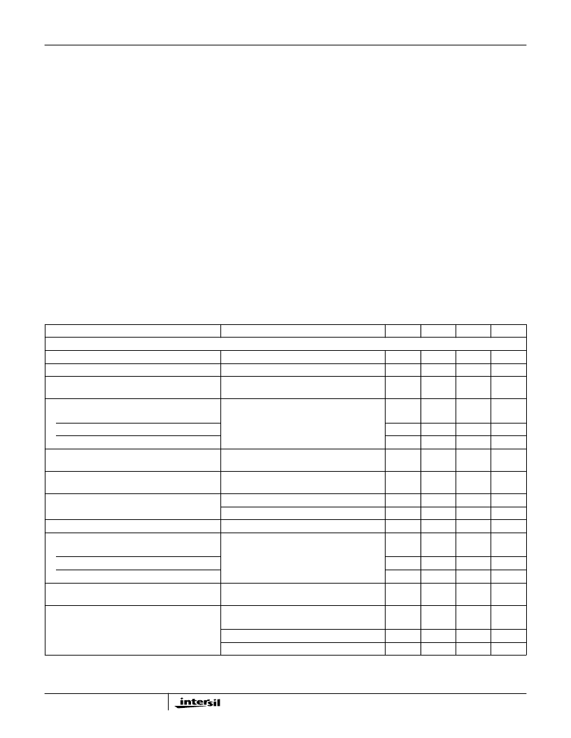
Electrical Specifications
Unless Otherwise Specified, Typical Parameters are at T
A
= 25
o
C, Min-Max Parameters are Over Operating
Temperature Range, V
B-
= -48V, V
B+
= 5V, AG = DG = BG = 0V. All AC Parameters are specified at 600
2-Wire Terminating Impedance
PARAMETER
TEST CONDITIONS
MIN
TYP
MAX
UNITS
AC TRANSMISSION PARAMETERS
RX Input Impedance
300Hz to 3.4kHz (Note 4)
-
100
-
k
TX Output Impedance
300Hz to 3.4kHz (Note 4)
-
-
20
4-Wire Input Overload Level
300Hz to 3.4kHz R
L
= 1200
,
600
Reference
Matched for 600
(Note 4)
1.5
-
-
V
PEAK
2-Wire Return Loss
SRL LO
26
35
-
dB
ERL
30
40
-
dB
SRL HI
30
40
-
dB
2-Wire Longitudinal to Metallic Balance
Off Hook
PerANSI/IEEESTD455-1976(Note4)300Hzto
3400Hz
58
63
-
dB
4-Wire Longitudinal Balance
Off Hook
300Hz to 3400Hz (Note 4)
50
55
-
dB
Low Frequency Longitudinal Balance
R.E.A. Test Circuit
I
LINE
= 40mA, T
A
= 25
o
C (Note 4)
I
LINE
= 40mA, T
A
= 25
o
C (Note 4)
0dBm at 1kHz, Referenced 600
-
-
-67
dBmp
-
-
23
dBrnC
Longitudinal Current Capability
-
-
30
mA
RMS
Insertion Loss
2-Wire/4-Wire
-
±
0.05
±
0.05
±
0.2
±
0.2
±
0.2
±
0.05
dB
4-Wire/2-Wire
-
dB
4-Wire/4-Wire
-
-
dB
Frequency Response
300Hz to 3400Hz (Note 4) Referenced to
Absolute Level at 1kHz, 0dBm Referenced 600
-
±
0.02
dB
Level Linearity
2-Wire to 4-Wire and 4-Wire to 2-Wire
Referenced to -10dBm (Note 4)
+3 to -40dBm
-
-
±
0.05
±
0.1
±
0.3
dB
-40 to -50dBm
-
-
dB
-50 to -55dBm
-
-
dB
HC-5509B
相關(guān)PDF資料 |
PDF描述 |
|---|---|
| HC1-5504DLC-5 | SLIC Subscriber Line Interface Circuit |
| HC1-5504DLC-9 | SLIC Subscriber Line Interface Circuit |
| HC1-5504B-5 | EIA/ITU PABX SLIC with 40mA Loop Feed |
| HC1-5504B-9 | EIA/ITU PABX SLIC with 40mA Loop Feed |
| HC4P5504B1- | ITU Low Cost, PABX SLIC With 40mA Loop Feed |
相關(guān)代理商/技術(shù)參數(shù) |
參數(shù)描述 |
|---|---|
| HC-5509B_03 | 制造商:INTERSIL 制造商全稱:Intersil Corporation 功能描述:ITU CO/Loop Carrier SLIC |
| HC5509B3 | 制造商:未知廠家 制造商全稱:未知廠家 功能描述:Telecommunication IC |
| HC-5509B3999-003 | 制造商:INTERSIL 制造商全稱:Intersil Corporation 功能描述:SLIC Subscriber Line Interface Circuit |
| HC5509B3999-003 | 制造商:未知廠家 制造商全稱:未知廠家 功能描述:Telecommunication IC |
| HC5509B4P | 制造商:未知廠家 制造商全稱:未知廠家 功能描述:Telecommunication IC |
發(fā)布緊急采購,3分鐘左右您將得到回復(fù)。