- 您現(xiàn)在的位置:買賣IC網(wǎng) > PDF目錄384385 > HA7210IBZ96 (INTERSIL CORP) 10kHz to 10MHz, Low Power Crystal Oscillator PDF資料下載
參數(shù)資料
| 型號(hào): | HA7210IBZ96 |
| 廠商: | INTERSIL CORP |
| 元件分類: | 模擬信號(hào)調(diào)理 |
| 英文描述: | 10kHz to 10MHz, Low Power Crystal Oscillator |
| 中文描述: | SPECIALTY ANALOG CIRCUIT, PDSO8 |
| 封裝: | PLASTIC, MS-012AA, SOIC-8 |
| 文件頁(yè)數(shù): | 4/15頁(yè) |
| 文件大?。?/td> | 321K |
| 代理商: | HA7210IBZ96 |
第1頁(yè)第2頁(yè)第3頁(yè)當(dāng)前第4頁(yè)第5頁(yè)第6頁(yè)第7頁(yè)第8頁(yè)第9頁(yè)第10頁(yè)第11頁(yè)第12頁(yè)第13頁(yè)第14頁(yè)第15頁(yè)
4
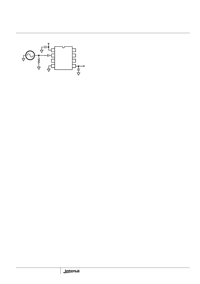
Test Circuit
In production the HA7210 is tested with a 32kHz and a
1MHz crystal. However for characterization purposes data
was taken using a sinewave generator as the frequency
determining element, as shown in Figure 1. The 1V
P-P
input
is a smaller amplitude than what a typical crystal would
generate so the transitions are slower. In general the
Generator data will show a “worst case” number for I
DD
,
duty cycle, and rise/fall time. The Generator test method is
useful for testing a variety of frequencies quickly and
provides curves which can be used for understanding
performance trends. Data for the HA7210 using crystals has
also been taken. This data has been overlaid onto the
generator data to provide a reference for comparison.
Application Information
Theory Of Operation
The HA7210 is a Pierce Oscillator optimized for low power
consumption, requiring no external components except for a
bypass capacitor and a Parallel Mode Crystal. The Simplified
Block Diagram shows the Crystal attached to pins 2 and 3, the
Oscillator input and output. The crystal drive circuitry is detailed
showing the simple CMOS inverter stage and the P-channel
device being used as biasing resistor R
F
. The inverter will
operate mostly in its linear region increasing the amplitude of
the oscillation until limited by its transconductance and voltage
rails, V
DD
and V
RN
. The inverter is self biasing using R
F
to
center the oscillating waveform at the input threshold. Do not
interfere with this bias function with external loads or excessive
leakage on pin 2. Nominal value for R
F
is 17M
in the lowest
frequency range to 7M
in the highest frequency range.
The HA7210 optimizes its power for 4 frequency ranges
selected by digital inputs Freq1 and Freq2 as shown in the
Block Diagram. Internal pull up resistors (constant current
0.4
μ
A) on Enable, Freq1 and Freq2 allow the user simply to
leave one or all digital inputs not connected for a
corresponding “1” state. All digital inputs may be left open for
10kHz to 100kHz operation.
A current source develops 4 selectable reference voltages
through series resistors. The selected voltage, V
RN
, is
buffered and used as the negative supply rail for the
oscillator section of the circuit. The use of a current source in
the reference string allows for wide supply variation with
minimal effect on performance. The reduced operating
voltage of the oscillator section reduces power consumption
and limits transconductance and bandwidth to the frequency
range selected. For frequencies at the edge of a range, the
higher range may provide better performance.
The OSC OUT waveform on pin 3 is squared up through a series
of inverters to the output drive stage. The Enable function is
implemented with a NAND gate in the inverter string, gating the
signal to the level shifter and output stage. Also during Disable
the output is set to a high impedance state useful for minimizing
power during standby and when multiple oscillators are OR’ed to
a single node.
Design Considerations
The low power CMOS transistors are designed to consume
power mostly during transitions. Keeping these transitions
short requires a good decoupling capacitor as close as
possible to the supply pins 1 and 4. A ceramic 0.1
μ
F is
recommended. Additional supply decoupling on the circuit
board with 1
μ
F to 10
μ
F will further reduce overshoot, ringing
and power consumption. The HA7210, when compared to a
crystal and inverter alone, will speed clock transition times,
reducing power consumption of all CMOS circuitry run from
that clock.
Power consumption may be further reduced by minimizing the
capacitance on moving nodes. The majority of the power will
be used in the output stage driving the load. Minimizing the
load and parasitic capacitance on the output, pin 5, will play
the major role in minimizing supply current. A secondary
source of wasted supply current is parasitic or crystal load
capacitance on pins 2 and 3. The HA7210 is designed to work
with most available crystals in its frequency range with no
external components required. Two 15pF capacitors are
internally switched onto crystal pins 2 and 3 on the HA7210 to
compensate the oscillator in the 10kHz to 100kHz frequency
range.
The supply current of the HA7210 may be approximately
calculated from the equation:
I
DD
= I
DD
(Disabled) + V
DD
×
f
OSC
×
C
L
where:
I
DD
= Total supply current
V
DD
= Total voltage from V
DD
(pin 1) to V
SS
(pin 4)
f
OSC
= Frequency of Oscillation
C
L
= Output (pin 5) load capacitance
EXAMPLE #1:
V
DD
= 5V, f
OSC
= 100kHz, C
L
= 30pF
I
DD
(Disabled) = 4.5
μ
A (Figure 10)
I
DD
= 4.5
μ
A + (5V)(100kHz)(30pF) = 19.5
μ
A
Measured I
DD
= 20.3
μ
A
EXAMPLE #2:
V
DD
= 5V, f
OSC
= 5MHz, C
L
= 30pF
I
DD
(Disabled) = 75
μ
A (Figure 9)
I
DD
= 75
μ
A + (5V)(5MHz)(30pF) = 825
μ
A
Measured I
DD
= 809
μ
A
1
2
3
4
8
7
6
5
HA7210
V
OUT
C
L
+5V
18pF
0.1
μ
F
1000pF
50
ENABLE
FREQ 2
FREQ 1
1V
P-P
FIGURE 1.
HA7210
相關(guān)PDF資料 |
PDF描述 |
|---|---|
| HA9P5320-5Z | 1 Microsecond Precision Sample and Hold Amplifier |
| HA9P5320-9 | 1 Microsecond Precision Sample and Hold Amplifier |
| HA-5320 | ECONOLINE: RxxP2xx - EN 60950 certified, rated for 250VAC - UL-60950-1 / CSA C22.2 certified - 5.2kVDC Isolation for 1 Minute - Optional Continuous Short Circuit Protected - Wide Operating Temperature Range at full 2 Watts Load, .40?????C to +85?????C - Twin Chamber Transform |
| HA9P5320-5 | 1 Microsecond Precision Sample and Hold Amplifier |
| HA-5320883 | High Speed Precision Sample and Hold Amplifier |
相關(guān)代理商/技術(shù)參數(shù) |
參數(shù)描述 |
|---|---|
| HA7210IP | 制造商:Rochester Electronics LLC 功能描述: |
| HA7210Y | 制造商:INTERSIL 制造商全稱:Intersil Corporation 功能描述:10kHz to 10MHz, Low Power Crystal Oscillator |
| HA7211IB | 制造商:Rochester Electronics LLC 功能描述:- Bulk |
| HA7211IB WAF | 制造商:Harris Corporation 功能描述: |
| HA7-2500/883 | 制造商:Rochester Electronics LLC 功能描述:PRECISION HIGH SLEW RATE OP AMP (30V/USEC) 8 CDIP MIL /883 - Bulk |
發(fā)布緊急采購(gòu),3分鐘左右您將得到回復(fù)。