- 您現(xiàn)在的位置:買賣IC網(wǎng) > PDF目錄384385 > HA5351IBZ (INTERSIL CORP) 64ns Sample and Hold Amplifier PDF資料下載
參數(shù)資料
| 型號: | HA5351IBZ |
| 廠商: | INTERSIL CORP |
| 元件分類: | 運動控制電子 |
| 英文描述: | 64ns Sample and Hold Amplifier |
| 中文描述: | SAMPLE AND HOLD AMPLIFIER, 90 us ACQUISITION TIME, PDSO8 |
| 封裝: | ROHS COMPLIANT, PLASTIC, MS-012AA, SOIC-8 |
| 文件頁數(shù): | 2/7頁 |
| 文件大小: | 182K |
| 代理商: | HA5351IBZ |
2
FN3690.10
April 12, 2007
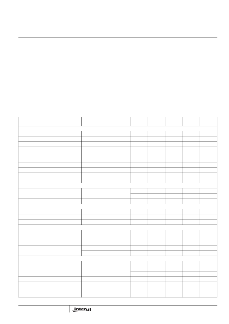
Absolute Maximum Ratings
Thermal Information
Voltage Between V+ and V- Terminals. . . . . . . . . . . . . . . . . . . .+11V
Differential Input Voltage . . . . . . . . . . . . . . . . . . . . . . . . . . . . . . . 6V
Voltage Between Sample and Hold Control and Ground. . . . . +5.5V
Output Current, Continuous. . . . . . . . . . . . . . . . . . . . . . . . . .
±
37mA
Operating Conditions
Temperature Range. . . . . . . . . . . . . . . . . . . . . . . . . .-40°C to +85°C
Thermal Resistance (Typical, Note 1)
SOIC Package . . . . . . . . . . . . . . . . . . . . . . . . . . . . .
Maximum Junction Temperature (Plastic Package) . . . . . . .+150°C
Maximum Storage Temperature Range. . . . . . . . . -65°C to +150°C
Pb-free reflow profile . . . . . . . . . . . . . . . . . . . . . . . . . .see link below
http://www.intersil.com/pbfree/Pb-FreeReflow.asp
θ
JA
(°C/W)
160
CAUTION: Stresses above those listed in “Absolute Maximum Ratings” may cause permanent damage to the device. This is a stress only rating and operation of the
device at these or any other conditions above those indicated in the operational sections of this specification is not implied.
NOTE:
1.
θ
JA
is measured with the component mounted on an evaluation PC board in free air.
Electrical Specifications
Test Conditions: V
SUPPLY
=
±
5V; C
H
= Internal = 15pF, Digital Input: V
IL
= 0V (Sample), V
IH
= 4.0V (Hold).
Non-Inverting Unity Gain Configuration (Output Tied to -Input), C
L
= 5pF,
Unless Otherwise Specified
PARAMETER
TEST CONDITIONS
TEMP.
(°C)
MIN
TYP
MAX
UNITS
INPUT CHARACTERISTICS
Input Voltage Range
Full
-2.5
-
+2.5
V
k
Ω
Input Resistance (Note 2)
25
100
500
-
Input Capacitance
25
-
-
5
pF
Input Offset Voltage
25
-2
-
2
mV
Full
-3.0
-
3.0
mV
μ
V/°C
μ
A
μ
A
Offset Voltage Temperature Coefficient
Full
-
15
-
Bias Current
Full
-
2.5
5
Offset Current
Full
-1.5
-
+1.5
Common Mode Range
Full
-2.5
-
+2.5
V
Common Mode Rejection Ratio
±
2.5V, Note 3
Full
60
80
-
dB
TRANSFER CHARACTERISTICS
Large Signal Voltage Gain
V
OUT
=
±
2.5V
25
95
108
-
dB
Full
85
-
-
dB
Unity Gain -3dB Bandwidth
25
-
40
-
MHz
TRANSIENT RESPONSE
Rise Time
200mV Step
25
-
8.5
-
ns
Overshoot
200mV Step
25
0
-
30
%
Slew Rate
5V Step
Full
88
105
-
V/
μ
s
DIGITAL INPUT CHARACTERISTICS
Input Voltage
V
IH
25, 85
2.1
-
5.0
V
-40
2.4
-
5.0
V
V
IL
V
IL
= 0V
V
IH
= 5V
Full
0
-
0.8
V
μ
A
μ
A
Input Current
Full
-1.0
-
1.0
Full
-1.0
-
1.0
OUTPUT CHARACTERISTICS
Output Voltage
R
L
= 510
Ω
R
L
= 100
Ω
Full
-3.0
-
+3.0
V
Output Current
25, 85
20
25
-
mA
-40
15
-
-
mA
Full Power Bandwidth
5V
P-P
, A
V
= +1, -3dB
Hold Mode
Full
-
13
-
MHz
Ω
μ
V
RMS
μ
V
RMS
Output Resistance
25
-
0.02
-
Total Output Noise
(DC to 10MHz)
Sample Mode
25
-
325
-
Hold Mode
25
-
325
-
HA5351
相關PDF資料 |
PDF描述 |
|---|---|
| HA5351 | 64ns Sample and Hold Amplifier(64ns級采樣保持放大器) |
| HA7210IBZ | 10kHz to 10MHz, Low Power Crystal Oscillator |
| HA7210IBZ96 | 10kHz to 10MHz, Low Power Crystal Oscillator |
| HA9P5320-5Z | 1 Microsecond Precision Sample and Hold Amplifier |
| HA9P5320-9 | 1 Microsecond Precision Sample and Hold Amplifier |
相關代理商/技術參數(shù) |
參數(shù)描述 |
|---|---|
| HA5351IP | 制造商:Rochester Electronics LLC 功能描述:SMP&HLD 40MHZ 64NS INTCAP 8PDIP IND - Bulk |
| HA-5351MJ/883 | 制造商:INTERSIL 制造商全稱:Intersil Corporation 功能描述:Fast Acquisition, Low Power Sample and Hold Amplifier |
| HA5352 | 制造商:INTERSIL 制造商全稱:Intersil Corporation 功能描述:Fast Acquisition Dual Sample and Hold Amplifier |
| HA5352/883 | 制造商:INTERSIL 制造商全稱:Intersil Corporation 功能描述:Fast Acquisition Dual Sample and Hold Amplifier |
| HA5352883 | 制造商:INTERSIL 制造商全稱:Intersil Corporation 功能描述:Fast Acquisition Dual Sample and Hold Amplifier |
發(fā)布緊急采購,3分鐘左右您將得到回復。