- 您現(xiàn)在的位置:買賣IC網(wǎng) > PDF目錄384385 > HA456CM (HARRIS SEMICONDUCTOR) 120MHz, Low Power, 8 x 8 Video Crosspoint Switch PDF資料下載
參數(shù)資料
| 型號: | HA456CM |
| 廠商: | HARRIS SEMICONDUCTOR |
| 元件分類: | 運(yùn)動控制電子 |
| 英文描述: | 120MHz, Low Power, 8 x 8 Video Crosspoint Switch |
| 中文描述: | 8-CHANNEL, CROSS POINT SWITCH, PQCC44 |
| 文件頁數(shù): | 4/15頁 |
| 文件大小: | 158K |
| 代理商: | HA456CM |
4
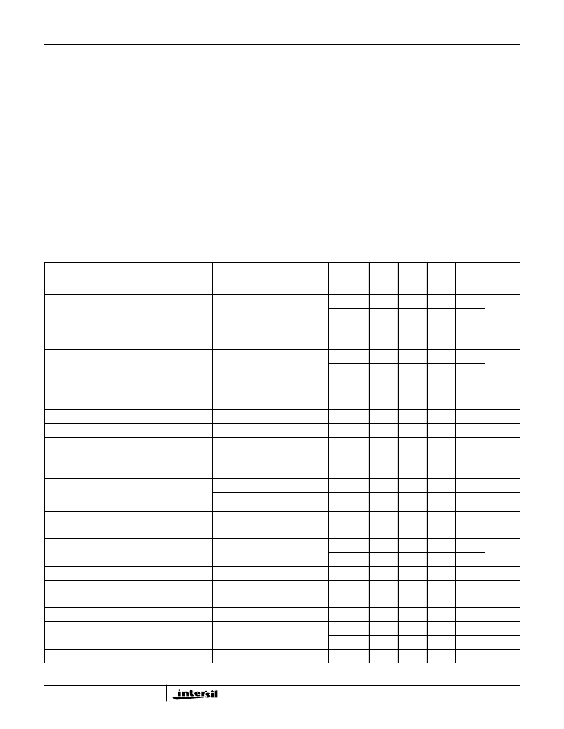
Absolute Maximum Ratings
Thermal Information
Supply Voltage (V+ to V-). . . . . . . . . . . . . . . . . . . . . . . . . . . . . . .12V
Positive Supply Voltage (V+) Referred to AGND . . . . . . . . . . . . . 6V
Negative Supply Voltage (V-) Referred to AGND. . . . . . . . . . . . -6V
DGND Voltage . . . . . . . . . . . . . . . . . . . . . . . . . . . . . . . . . AGND
±
1V
Analog Input Voltage
. . . . . . . . . . . . . . . . . . . . . . . . . . . . . . . .±
V
SUPPLY
Digital Input Voltage. . . . . . . . . . . . . . (V+ + 0.3V) to (DGND - 0.3V)
ESD Rating
Human Body Model (Per MIL-STD-883 Method 3015.7). . . . 1.5kV
Operating Conditions
Temperature Range. . . . . . . . . . . . . . . . . . . . . . . . . . . .0
o
C to 70
o
C
Supply Voltage Range (Typical)
. . . . . . . . . . . . . . . . . . .±
4.5V to
±
5.5V
Thermal Resistance (Typical, Note 1)
PLCC Package. . . . . . . . . . . . . . . . . . . . . . . . . . . . .
MQFP Package . . . . . . . . . . . . . . . . . . . . . . . . . . . .
Moisture Sensitivity (see Technical Brief TB363)
PLCC Package. . . . . . . . . . . . . . . . . . . . . . . . . . . . . . . . . . Level 1
MQFP Package . . . . . . . . . . . . . . . . . . . . . . . . . . . . . . . . . Level 3
Maximum Junction Temperature (Die). . . . . . . . . . . . . . . . . . .175
o
C
Maximum Junction Temperature (Plastic Package). . . . . . . . .150
o
C
Maximum Storage Temperature Range. . . . . . . . . . -65
o
C to 150
o
C
Maximum Lead Temperature (Soldering 10s) . . . . . . . . . . . . .300
o
C
(Lead Tips Only)
θ
JA
(
o
C/W)
50
70
CAUTION: Stresses above those listed in “Absolute Maximum Ratings” may cause permanent damage to the device. This is a stress only rating and operation of the
device at these or any other conditions above those indicated in the operational sections of this specification is not implied.
NOTE:
1.
θ
JA
is measured with the component mounted on an evaluation PC board in free air.
Electrical Specifications
V
SUPPLY
=
±
5V, AGND = DGND = 0V, R
L
= 400
(
Note 2)
,
Unless Otherwise Specified.
PARAMETER
TEST CONDITIONS
(NOTE 3)
TEST
LEVEL
TEMP
(
o
C)
MIN
TYP
MAX
UNITS
Voltage Gain
V
IN
= -1.5V to +1.5V, Worst Case
Switch Configuration
A
25
0.992
0.996
1.00
V/V
A
Full
0.99
0.995
1.00
Channel-to-Channel Gain Mismatch
A
25
-
0.001
0.004
V/V
A
Full
-
0.001
0.005
Supply Current
All Outputs Enabled, R
L
= Open,
V
IN
= 0V,
Total for All V+ (3) or V- (2) Pins
A
25
-
68
80
mA
A
Full
-
71
83
Disabled Supply Current
All Outputs Disabled, R
L
= Open,
Total for All V+ (3) or V- (2) Pins
A
25
-
47
65
mA
A
Full
-
47
67
Input Voltage Range
A
Full
±
2
±
2.5
-
V
Analog Input Current
V
IN
= 0V
DC to 40MHz
A
Full
-
1.6
12
μ
A
Input Noise (R
S
= 75
)
B
25
-
0.15
-
mV
RMS
nV/
√
Hz
≥
10kHz
B
25
-
22
-
Analog Input Resistance
DC
C
25
-
4
-
M
Analog Input Capacitance (Input
Connected to One Output or All Outputs,
Note 6)
PLCC Package
B
25
-
3.2
-
pF
MQFP Package
B
25
-
2.5
-
pF
Output Offset Voltage
V
IN
= 0V, Worst Case Switch
Configuration
A
25
-18
-6.5
5
mV
A
Full
-20
-7.5
6
Channel-to-Channel Offset Voltage
Mismatch
A
25
-
2
11
mV
A
Full
-
4
13
Offset Voltage Drift
B
Full
-
20
-
μ
V/
o
C
Output Voltage Swing
V
IN
=
±
2.5V
A
25
±
2.2
±
2.48
-
V
A
Full
±
2.1
±
2.47
-
V
Output Resistance
Enabled, DC
B
25
-
0.25
-
Output Leakage Current
(Including D1/SER OUT)
All Outputs Disabled,
V
OUT
= 2.5V
A
25
-
0.2
5
μ
A
A
Full
-
1
10
μ
A
Output Resistance
Output Disabled
A
25
0.6
15
-
M
HA456
相關(guān)PDF資料 |
PDF描述 |
|---|---|
| HA456CN | 120MHz, Low Power, 8 x 8 Video Crosspoint Switch |
| HA456 | 120MHz, Low Power, 8 x 8 Video Crosspoint Switch |
| HA4600CBZ | 480MHz, SOT-23, Video Buffer with Output Disable |
| HA4600CBZ96 | 480MHz, SOT-23, Video Buffer with Output Disable |
| HA4600CHZ96 | 480MHz, SOT-23, Video Buffer with Output Disable |
相關(guān)代理商/技術(shù)參數(shù) |
參數(shù)描述 |
|---|---|
| HA456CMZ | 功能描述:模擬和數(shù)字交叉點(diǎn) IC W/ANNEAL XPOINT 8X8 VID GAIN+1 44PLCC RoHS:否 制造商:Micrel 配置:2 x 2 封裝 / 箱體:MLF-16 數(shù)據(jù)速率:10.7 Gbps 輸入電平:CML, LVDS, LVPECL 輸出電平:CML 電源電壓-最大:3.6 V 電源電壓-最小:2.375 V 最大工作溫度:+ 85 C 最小工作溫度:- 40 C 產(chǎn)品:Digital Crosspoint 封裝:Tube |
| HA456CN | 制造商:Rochester Electronics LLC 功能描述:XPOINT 8X8 VIDEO GAIN+1 44MQFP COM - Bulk |
| HA456CP | 制造商:Rochester Electronics LLC 功能描述:- Bulk |
| HA456EVAL1 | 功能描述:交換機(jī) IC 開發(fā)工具 EVAL PLATFORM HA456 RoHS:否 制造商:Maxim Integrated 產(chǎn)品:Evaluation Kits 類型:USB Power Switches 工具用于評估:MAX4984E 工作電源電壓:2.8 V to 5.5 V |
| HA457 | 制造商:INTERSIL 制造商全稱:Intersil Corporation 功能描述:95MHz, Low Power, AV = 2, 8 x 8 Video Crosspoint Switch |
發(fā)布緊急采購,3分鐘左右您將得到回復(fù)。