- 您現(xiàn)在的位置:買賣IC網(wǎng) > PDF目錄384385 > HA4314BCP (HARRIS SEMICONDUCTOR) 400MHz, 4 x 1 Video Crosspoint Switch PDF資料下載
參數(shù)資料
| 型號(hào): | HA4314BCP |
| 廠商: | HARRIS SEMICONDUCTOR |
| 元件分類: | 運(yùn)動(dòng)控制電子 |
| 英文描述: | 400MHz, 4 x 1 Video Crosspoint Switch |
| 中文描述: | 4-CHANNEL, CROSS POINT SWITCH, PDIP14 |
| 文件頁(yè)數(shù): | 2/10頁(yè) |
| 文件大小: | 127K |
| 代理商: | HA4314BCP |
2
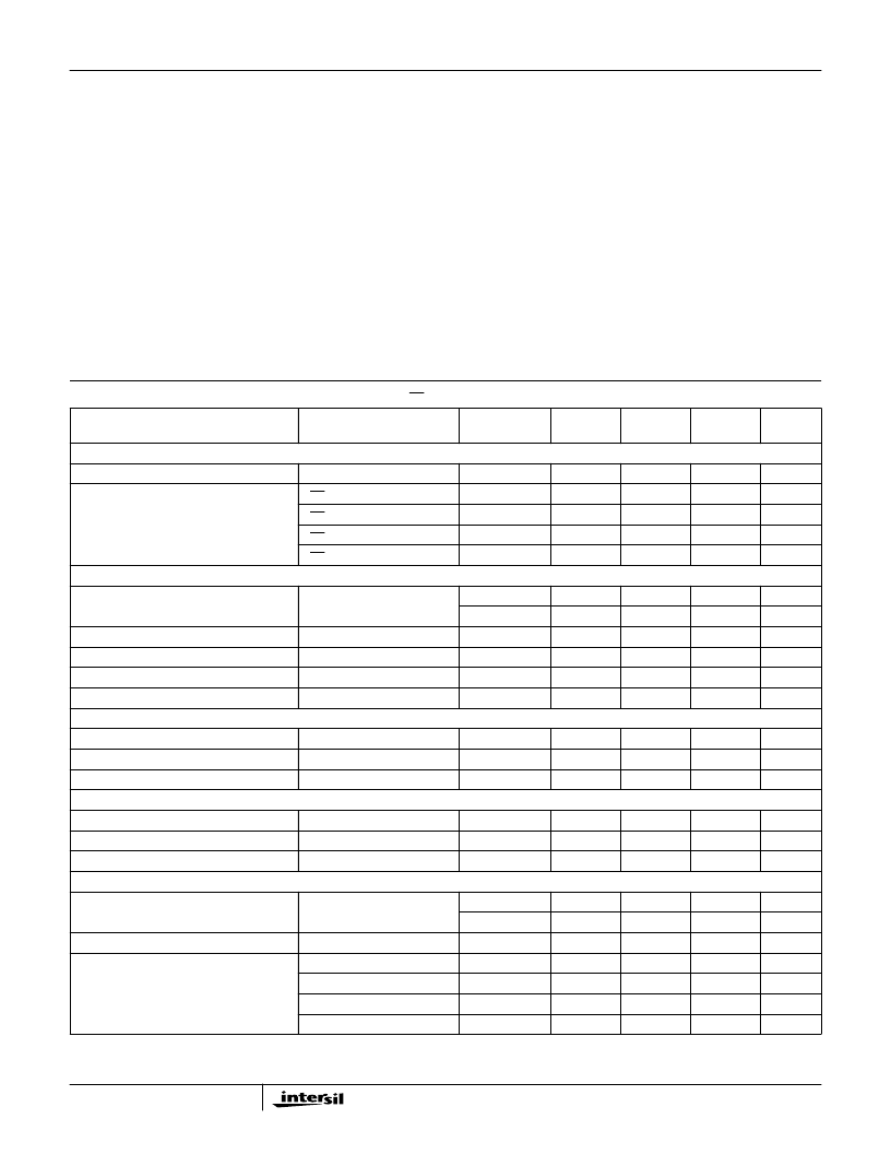
Absolute Maximum Ratings
Thermal Information
Voltage Between V+ and V- . . . . . . . . . . . . . . . . . . . . . . . . . . . . 12V
Input Voltage . . . . . . . . . . . . . . . . . . . . . . . . . . . . . . . . . . . V
SUPPLY
Digital Input Current (Note 2). . . . . . . . . . . . . . . . . . . . . . . . .
±
25mA
Analog Input Current (Note 2) . . . . . . . . . . . . . . . . . . . . . . . . .
±
5mA
Output Current. . . . . . . . . . . . . . . . . . . . . . . . . . . . . . . . . . . . . 20mA
ESD Rating
Human Body Model (Per MIL-STD-883 Method 3015.7). . . .2000V
Operating Conditions
Temperature Range. . . . . . . . . . . . . . . . . . . . . . . . . . . 0
o
C to 70
o
C
Thermal Resistance (Typical, Note 1)
PDIP Package . . . . . . . . . . . . . . . . . . . . . . . . . . . . .
SOIC Package . . . . . . . . . . . . . . . . . . . . . . . . . . . . .
SSOP Package . . . . . . . . . . . . . . . . . . . . . . . . . . . .
Maximum Junction Temperature (Die) . . . . . . . . . . . . . . . . . . . 175
o
C
Maximum Junction Temperature (Plastic Package) . . . . . . . 150
o
C
Maximum Storage Temperature Range. . . . . . . . . . -65
o
C to 150
o
C
Maximum Lead Temperature (Soldering 10s) . . . . . . . . . . . . 300
o
C
(SOIC and SSOP - Lead Tips Only)
θ
JA
(
o
C/W)
100
120
140
CAUTION: Stresses above those listed in “Absolute Maximum Ratings” may cause permanent damage to the device. This is a stress only rating and operation of the
device at these or any other conditions above those indicated in the operational sections of this specification is not implied.
NOTES:
1.
θ
JA
is measured with the component mounted on an evaluation PC board in free air.
2. If an input signal is applied before the supplies are powered up, the input current must be limited to these maximum values.
Electrical Specifications
V
SUPPLY
=
±
5V, R
L
= 10k
, V
CS
= 0.8V, Unless Otherwise Specified
PARAMETER
TEST CONDITIONS
(NOTE 4)
TEMP. (
o
C)
MIN
TYP
MAX
UNITS
DC SUPPLY CHARACTERISTICS
Supply Voltage
Full
±
4.5
±
5.0
±
5.5
V
Supply Current (V
OUT
= 0V)
V
CS
= 0.8V
V
CS
= 0.8V
V
CS
= 2.0V
V
CS
= 2.0V
25, 70
-
10.5
13
mA
0
-
-
15.5
mA
25, 70
-
400
450
μ
A
μ
A
0
-
400
580
ANALOG DC CHARACTERISTICS
Output Voltage Swing without Clipping
V
OUT
= V
IN
±
V
IO
±
20mV
25, 70
±
2.7
±
2.4
±
2.8
±
2.5
-
V
0
-
V
Output Current
Full
15
20
-
mA
Input Bias Current
Full
-
30
50
μ
A
Output Offset Voltage
Full
-10
-
10
mV
μ
V/
o
C
Output Offset Voltage Drift (Note 3)
Full
-
25
50
SWITCHING CHARACTERISTICS
Turn-On Time
25
-
160
-
ns
Turn-Off Time
25
-
320
-
ns
Output Glitch During Switching
25
-
±
10
-
mV
DIGITAL DC CHARACTERISTICS
Input Logic High Voltage
Full
2
-
-
V
Input Logic Low Voltage
Full
-
-
0.8
V
Input Current
0V to 4V
Full
-2
-
2
μ
A
AC CHARACTERISTICS
Insertion Loss
1V
P-P
25
-
0.055
0.063
dB
Full
-
0.07
0.08
dB
Channel-to-Channel Insertion Loss Match
Full
-
±
0.004
±
0.006
dB
-3dB Bandwidth
R
S
= 50
, C
L
= 10pF
R
S
= 20
, C
L
= 20pF
R
S
= 16
, C
L
= 36pF
R
S
= 13
, C
L
= 49pF
25
-
400
-
MHz
25
-
280
-
MHz
25
-
140
-
MHz
25
-
110
-
MHz
HA4314B
相關(guān)PDF資料 |
PDF描述 |
|---|---|
| HA4314BCA | 400MHz, 4 x 1 Video Crosspoint Switch |
| HA4314BCA96 | 400MHz, 4 x 1 Video Crosspoint Switch |
| HA4314BCB96 | 400MHz, 4 x 1 Video Crosspoint Switch |
| HA4314B | 400MHz, 4x1 Video Crosspoint Switch(400MHz,4x1 視頻矩陣開關(guān)) |
| HA4344BCBZ | 350MHz, 4x1 Video Crosspoint Switch with Synchronous Controls |
相關(guān)代理商/技術(shù)參數(shù) |
參數(shù)描述 |
|---|---|
| HA4314BCPZ | 功能描述:模擬和數(shù)字交叉點(diǎn) IC W/ANNEAL MUX 4:1 VID COM RoHS:否 制造商:Micrel 配置:2 x 2 封裝 / 箱體:MLF-16 數(shù)據(jù)速率:10.7 Gbps 輸入電平:CML, LVDS, LVPECL 輸出電平:CML 電源電壓-最大:3.6 V 電源電壓-最小:2.375 V 最大工作溫度:+ 85 C 最小工作溫度:- 40 C 產(chǎn)品:Digital Crosspoint 封裝:Tube |
| HA4314CB96 | 制造商:未知廠家 制造商全稱:未知廠家 功能描述:Interface IC |
| HA4344 | 制造商:INTERSIL 制造商全稱:Intersil Corporation 功能描述:350MHz, 4 x 1 Video Crosspoint Switch with Synchronous Controls |
| HA4344B | 制造商:INTERSIL 制造商全稱:Intersil Corporation 功能描述:350MHz, 4x1 Video Crosspoint Switch with Synchronous Controls |
| HA4344B_06 | 制造商:INTERSIL 制造商全稱:Intersil Corporation 功能描述:350MHz, 4x1 Video Crosspoint Switch with Synchronous Controls |
發(fā)布緊急采購(gòu),3分鐘左右您將得到回復(fù)。