- 您現(xiàn)在的位置:買賣IC網(wǎng) > PDF目錄384385 > HA1-5330-2 (HARRIS SEMICONDUCTOR) 650ns Precision Sample and Hold Amplifier PDF資料下載
參數(shù)資料
| 型號: | HA1-5330-2 |
| 廠商: | HARRIS SEMICONDUCTOR |
| 元件分類: | 運(yùn)動控制電子 |
| 英文描述: | 650ns Precision Sample and Hold Amplifier |
| 中文描述: | SAMPLE AND HOLD AMPLIFIER, 0.65 us ACQUISITION TIME, CDIP14 |
| 文件頁數(shù): | 2/5頁 |
| 文件大小: | 63K |
| 代理商: | HA1-5330-2 |
2
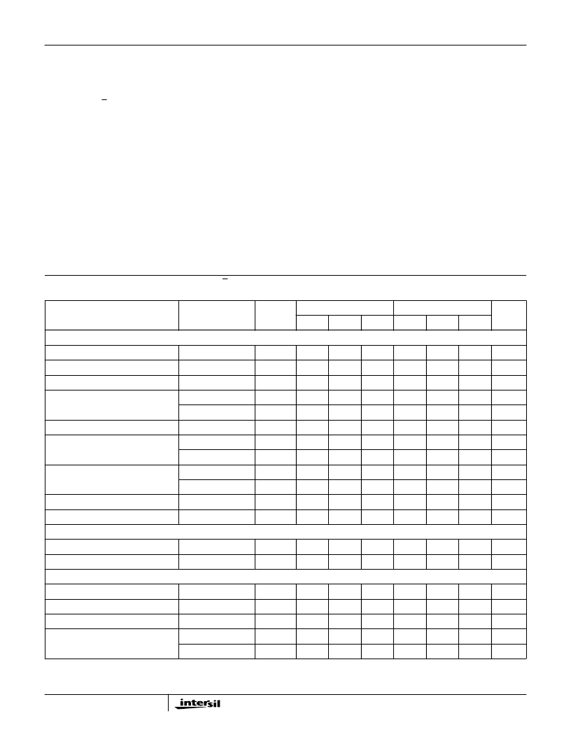
Absolute Maximum Ratings
Thermal Information
Voltage between V+ and SUPPLY/SIG GND. . . . . . . . . . . . . . +20V
Voltage between V- and SUPPLY/SIG GND . . . . . . . . . . . . . . . -20V
Voltage between SUPPLY GND and SIG GND . . . . . . . . . . . .
±
2.0V
Voltage between S/H Control and SUPPLY/SIG GND. . . . +8V, -6V
Differential Input Voltage . . . . . . . . . . . . . . . . . . . . . . . . . . . . . . 24V
Output Current, Continuous (Note 1). . . . . . . . . . . . . . . . . . .
±
17mA
Operating Conditions
Temperature Range
HA-5330-2 . . . . . . . . . . . . . . . . . . . . . . . . . . . . . . -55
o
C to 125
o
C
HA-5330-5 . . . . . . . . . . . . . . . . . . . . . . . . . . . . . . . . 0
o
C to 75
o
C
Supply Voltage Range (Typical). . . . . . . . . . . . . . . . .
±
10V to
±
20V
Thermal Resistance (Typical, Note 3)
CERDIP Package. . . . . . . . . . . . . . . . .
PDIP Package . . . . . . . . . . . . . . . . . . .
Maximum Junction Temperature (Ceramic Package, Note 2) . . .175
o
C
Maximum Junction Temperature (Plastic Package) . . . . . . . .150
o
C
Maximum Storage Temperature Range. . . . . . . . . . -65
o
C to 150
o
C
Maximum Lead Temperature (Soldering 10s) . . . . . . . . . . . . 300
o
C
θ
JA
(
o
C/W)
66
90
θ
JC
(
o
C/W)
16
N/A
CAUTION: Stresses above those listed in “Absolute Maximum Ratings” may cause permanent damage to the device. This is a stress only rating and operation of the
device at these or any other conditions above those indicated in the operational sections of this specification is not implied.
NOTES:
1. Internal Power Dissipation may limit Output Current below
±
17mA.
2. Maximumpowerdissipation,includingoutputload,mustbedesignedtomaintainthejunctiontemperaturebelow175
o
Cfortheceramicpackage,
and below 150
o
C for the plastic package.
3.
θ
JA
is measured with the component mounted on an evaluation PC board in free air.
Electrical Specifications
V
SUPPLY
=
±
15V; S/H Control V
IL
= +0.8V (Sample): V
IH
= +2.0V (Hold); SIG GND = SUPPLY GND,
Unity Gain Configuration (Output tied to -Input), Unless Otherwise Specified
PARAMETER
TEST
CONDITIONS
TEMP.
(
o
C)
HA-5330-2
HA-5330-5
UNITS
MIN
TYP
MAX
MIN
TYP
MAX
INPUT CHARACTERISTICS
Input Voltage Range
Full
±
10
-
-
±
10
-
-
V
Input Resistance (Note 4)
25
5
15
-
5
15
-
M
Input Capacitance
25
-
3
-
-
3
-
pF
Offset Voltage
25
-
0.2
-
-
0.2
-
mV
Full
-
-
2.0
-
-
1.5
mV
Offset Voltage Temperature Coefficient
Full
-
1
10
-
1
10
μ
V/
o
C
Bias Current
25
-
±
20
-
-
±
20
-
nA
Full
-
-
±
500
-
-
±
300
nA
Offset Current
25
-
20
-
-
20
-
nA
Full
-
-
500
-
-
300
nA
Common Mode Range
Full
±
10
-
-
±
10
-
-
V
CMRR
V
CM
=
±
10V
Full
86
100
-
86
100
-
dB
TRANSFER CHARACTERISTICS
Gain
DC
Full
2 x 10
6
2 x 10
7
-
2 x 10
6
2 x 10
7
-
V/V
Gain Bandwidth Product
Note 12
25
-
4.5
-
-
4.5
-
MHz
OUTPUT CHARACTERISTICS
Output Voltage
Full
±
10
-
-
±
10
-
-
V
Output Current
Full
±
10
-
-
±
10
-
-
mA
Full Power Bandwidth (Note 6)
25
-
1.4
-
-
1.4
-
MHz
Output Resistance
Hold Mode
25
-
0.2
-
-
0.2
-
Sample Mode
25
-
10
-5
0.001
-
10
-5
0.001
HA-5330
相關(guān)PDF資料 |
PDF描述 |
|---|---|
| HA1-5330-5 | 650ns Precision Sample and Hold Amplifier |
| HA2-5160-2 | 100MHz, JFET Input, High Slew Rate, Uncompensated, Operational Amplifier |
| HA2-5160-5 | 100MHz, JFET Input, High Slew Rate, Uncompensated, Operational Amplifier |
| HA-5160 | 100MHz, JFET Input, High Slew Rate, Uncompensated, Operational Amplifier |
| HA2-5170-5 | 8MHz, Precision, JFET Input Operational Amplifier |
相關(guān)代理商/技術(shù)參數(shù) |
參數(shù)描述 |
|---|---|
| HA1-5330-4 | 制造商:Rochester Electronics LLC 功能描述:- Bulk |
| HA1-5330-5 | 功能描述:采樣&保持放大器 SMP&HLD 4 5MHZ 650NS INTCAP 14CDIP COM RoHS:否 制造商:Texas Instruments 通道數(shù)量:2 捕獲時間:20 us 電源電壓-最大:18 V 最大工作溫度:+ 85 C 最小工作溫度:- 25 C 安裝風(fēng)格: 封裝 / 箱體:SOIC-14 封裝:Tube |
| HA1-5340 DIE | 制造商:Harris Corporation 功能描述: |
| HA1-5340/883 | 制造商:Rochester Electronics LLC 功能描述:- Bulk |
| HA1-5340-5 | 制造商:Rochester Electronics LLC 功能描述:- Bulk |
發(fā)布緊急采購,3分鐘左右您將得到回復(fù)。