- 您現(xiàn)在的位置:買賣IC網(wǎng) > PDF目錄362686 > EM78M612CBM (ELAN Microelctronics Corp .) Universal Serial Bus Microcontroller Series PDF資料下載
參數(shù)資料
| 型號(hào): | EM78M612CBM |
| 廠商: | ELAN Microelctronics Corp . |
| 英文描述: | Universal Serial Bus Microcontroller Series |
| 中文描述: | 通用串行總線控制器系列 |
| 文件頁數(shù): | 32/38頁 |
| 文件大小: | 1264K |
| 代理商: | EM78M612CBM |
第1頁第2頁第3頁第4頁第5頁第6頁第7頁第8頁第9頁第10頁第11頁第12頁第13頁第14頁第15頁第16頁第17頁第18頁第19頁第20頁第21頁第22頁第23頁第24頁第25頁第26頁第27頁第28頁第29頁第30頁第31頁當(dāng)前第32頁第33頁第34頁第35頁第36頁第37頁第38頁
EM78M612
Universal Serial Bus Microcontroller Series
This specification may change without further notice
.
2004/4/28 V1.1
32
Detecting block will start to sample the P60 input signal and measure the high pulse or low
pulse width. After detecting the transition of this signal and debouncing, the value of the
counter will be loaded into the RA (if the signal is transiting from high to low) or RB (if the
signal is transiting from low to high), and the counter is cleared to start counting from zero.
Two interrupts are supported individually by RA and RB. After the PDA function is enabled
(by setting IOCE[2] to 1), a default value is written to the High Pattern counter register and
Low Pattern counter register. Then define the corresponding interrupt enable bits (IOCF[6]
and IOCF[7]). When the counter value of one “H” pattern is bigger than the RA default value,
then the High Pattern Detecting interrupt will be generated. Similarly, if the counter value of
one “L” pattern is bigger than the RB default value, the Low Pattern Detecting interrupt will
occur. Then, the EM78M612 will be notified that one successful pattern is received from P60.
If these two interrupts are not used, they can be masked. The new counter value of a pattern
will still be loaded to the RA and RB. The firmware must be made to poll and determines any
changes to the value of these two registers.
The sample clock is programmable with 8 frequencies to choose from.
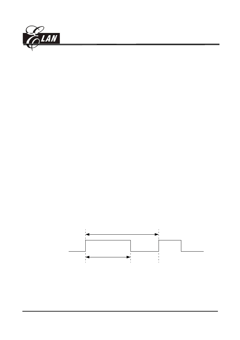
8.9 Pulse Width Modulation (PWM)
8.9.1 Function Description
In PWM mode, both of PWM1 (P64) and PWM2 (P65) produce up to a 8-bit resolution PWM
output. PWM output has a duty cycle and keeps the output high.
The PWM Period is defined as
0xFF * Timer Counter Clock
. The Timer Counter clock
source is controlled by Control Register IOC8S. For example; if the Clock source is 1MHz,
then the Period will be 255
μ
seconds.
Period = 255 * (1/Timer Counter Clock)
Period (0xFF * Clock)
Duty Cycle
Fig.8.9.2 The PWM Output Timing
The PWM duty cycle is defined by writing to the R8S/R9S Register for PWM1/PWM2.
Duty Cycle = R8S * (1/Timer Counter Clock) for PWM1
R9S * (1/Timer Counter Clock) for PWM2
相關(guān)PDF資料 |
PDF描述 |
|---|---|
| EM78M612CBP | Universal Serial Bus Microcontroller Series |
| EM78M612CCM | Universal Serial Bus Microcontroller Series |
| EM78M612CCP | Universal Serial Bus Microcontroller Series |
| EM78M612CDM | Universal Serial Bus Microcontroller Series |
| EM78M612CFM | Universal Serial Bus Microcontroller Series |
相關(guān)代理商/技術(shù)參數(shù) |
參數(shù)描述 |
|---|---|
| EM78M612CBP | 制造商:EMC 制造商全稱:ELAN Microelectronics Corp 功能描述:Universal Serial Bus Microcontroller Series |
| EM78M612CCM | 制造商:EMC 制造商全稱:ELAN Microelectronics Corp 功能描述:Universal Serial Bus Microcontroller Series |
| EM78M612CCP | 制造商:EMC 制造商全稱:ELAN Microelectronics Corp 功能描述:Universal Serial Bus Microcontroller Series |
| EM78M612CDM | 制造商:EMC 制造商全稱:ELAN Microelectronics Corp 功能描述:Universal Serial Bus Microcontroller Series |
| EM78M612CDP | 制造商:EMC 制造商全稱:ELAN Microelectronics Corp 功能描述:Universal Serial Bus Microcontroller Series |
發(fā)布緊急采購,3分鐘左右您將得到回復(fù)。