- 您現(xiàn)在的位置:買賣IC網(wǎng) > PDF目錄384294 > EM424M1622VTA (Electronic Theatre Controls, Inc.) 16Mb ( 2Banks ) Synchronous DRAM PDF資料下載
Rev.01
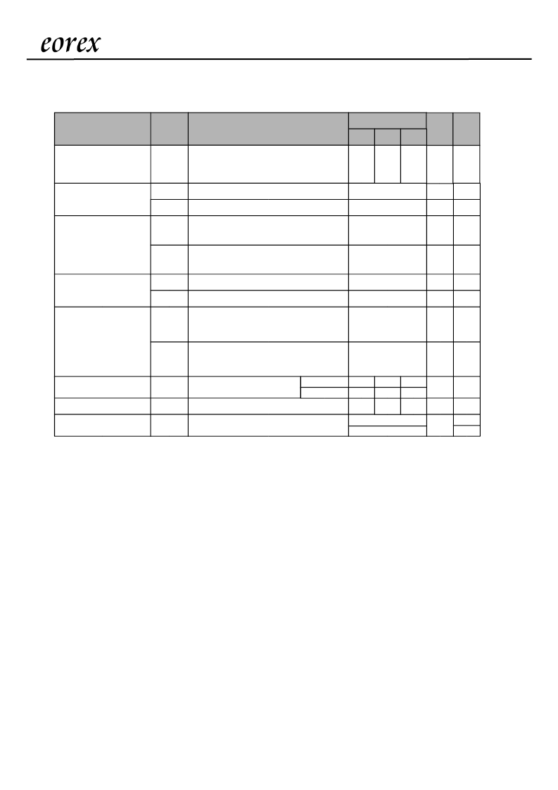
16Mb SDRAM
15/18
Recommended DC Operating Conditions
( VDD = 3.3V +/- 0.3 V, Ta = 0 ~ 70 °C , Ta = -40 to 85°C for 6I)
Note :
1. ICC1 depends on output loading and cycle rates.
Specified values are obtained w ith the output open.
Input signals are changed only one time during tCK(min)
2. ICC4 depends on output loading and cycle rates.
Specified values are obtained w ith the output open.
Input signals are changed only one time during tCK(min)
3. Input signals are changed only one time during tCK(min)
4. Standard pow er version.
5. * Low pow er version.
Precharge standby
current in power down
mode
Precharge standby
current in non-power
down mode
Active standby current
in non-power down
mode
operating current
(Burst mode)
Refresh current
Self Refresh current
Active standby current
in power down mode
mA
mA
CKE
≥
V
IL
(min), t
CK
= 15ns,/ CS
≥
V
IH
(min)
Input signals are changed one time during
30ns
CKE
≥
V
IL
(min), t
CK
=
∞
Input signals are stable
I
CC3N
I
CC3NS
30
20
CKE
≤
V
IL
(max.), t
Ck
=
∞
Operating current
Parameter
Test condition
Burst length = 1,
t
RC
≥
t
RC
(min), IOL = 0 mA,
One bank active
CKE
≤
V
IL
(max.), t
Ck
= 15 ns
Symbol
I
CC1
I
CC2P
I
CC2PS
MAX
100
5
2 / 0.7*
2 / 0.7*
mA
mA
Units
mA
Notes
1
5
5
90
6/6I/6L
80
7/7L
CKE
≥
V
IL
(min.), t
CK
= 15 ns, /CS
≥
V
IH
(min.)
Input signals are changed one time during 30ns
CKE
≥
V
IL
(min.), t
CK
=
∞
Input signals are stable
I
CC2N
I
CC2NS
20
8
mA
mA
mA
mA
mA
2
3
4
5
t
CCD
= 2CLKs , I
OL
= 0 mA
t
RC
≥
t
RC
(min.)
CKE
≤
0.2V
I
CC4
I
CC5
I
CC6
130
2
120
180
160
140
110
mA
mA
CKE
≤
V
IL
(max), t
CK
= 15ns
CKE
≤
V
IL
(max), t
CK
=
∞
I
CC3P
I
CC3PS
5
5
0.3
CL=3
CL=2
相關(guān)PDF資料 |
PDF描述 |
|---|---|
| EM424M1622VTB | 16Mb ( 2Banks ) Synchronous DRAM |
| EM424M1624VTA | 16Mb ( 2Banks ) Synchronous DRAM |
| EM424M1624VTB | 16Mb ( 2Banks ) Synchronous DRAM |
| EM424M812VTA | 16Mb ( 2Banks ) Synchronous DRAM |
| EM424M812VTB | 16Mb ( 2Banks ) Synchronous DRAM |
相關(guān)代理商/技術(shù)參數(shù) |
參數(shù)描述 |
|---|---|
| EM424M1622VTB | 制造商:未知廠家 制造商全稱:未知廠家 功能描述:16Mb ( 2Banks ) Synchronous DRAM |
| EM424M1624VTA | 制造商:未知廠家 制造商全稱:未知廠家 功能描述:16Mb ( 2Banks ) Synchronous DRAM |
| EM424M1624VTB | 制造商:未知廠家 制造商全稱:未知廠家 功能描述:16Mb ( 2Banks ) Synchronous DRAM |
| EM424M1644RTA-5FE | 制造商:EOREX 制造商全稱:EOREX 功能描述:128Mb (2M】4Bank】16) Double DATA RATE SDRAM |
| EM424M1644RTA-6FE | 制造商:EOREX 制造商全稱:EOREX 功能描述:128Mb (2M】4Bank】16) Double DATA RATE SDRAM |
發(fā)布緊急采購,3分鐘左右您將得到回復(fù)。