- 您現(xiàn)在的位置:買賣IC網(wǎng) > PDF目錄116211 > 531FC547M000DG (SILICON LABORATORIES) CRYSTAL OSCILLATOR, CLOCK, 547 MHz, LVDS OUTPUT PDF資料下載
參數(shù)資料
| 型號: | 531FC547M000DG |
| 廠商: | SILICON LABORATORIES |
| 元件分類: | XO, clock |
| 英文描述: | CRYSTAL OSCILLATOR, CLOCK, 547 MHz, LVDS OUTPUT |
| 封裝: | ROHS COMPLIANT, SMD, 6 PIN |
| 文件頁數(shù): | 7/12頁 |
| 文件大小: | 215K |
| 代理商: | 531FC547M000DG |
Si530/531
4
Rev. 1.1
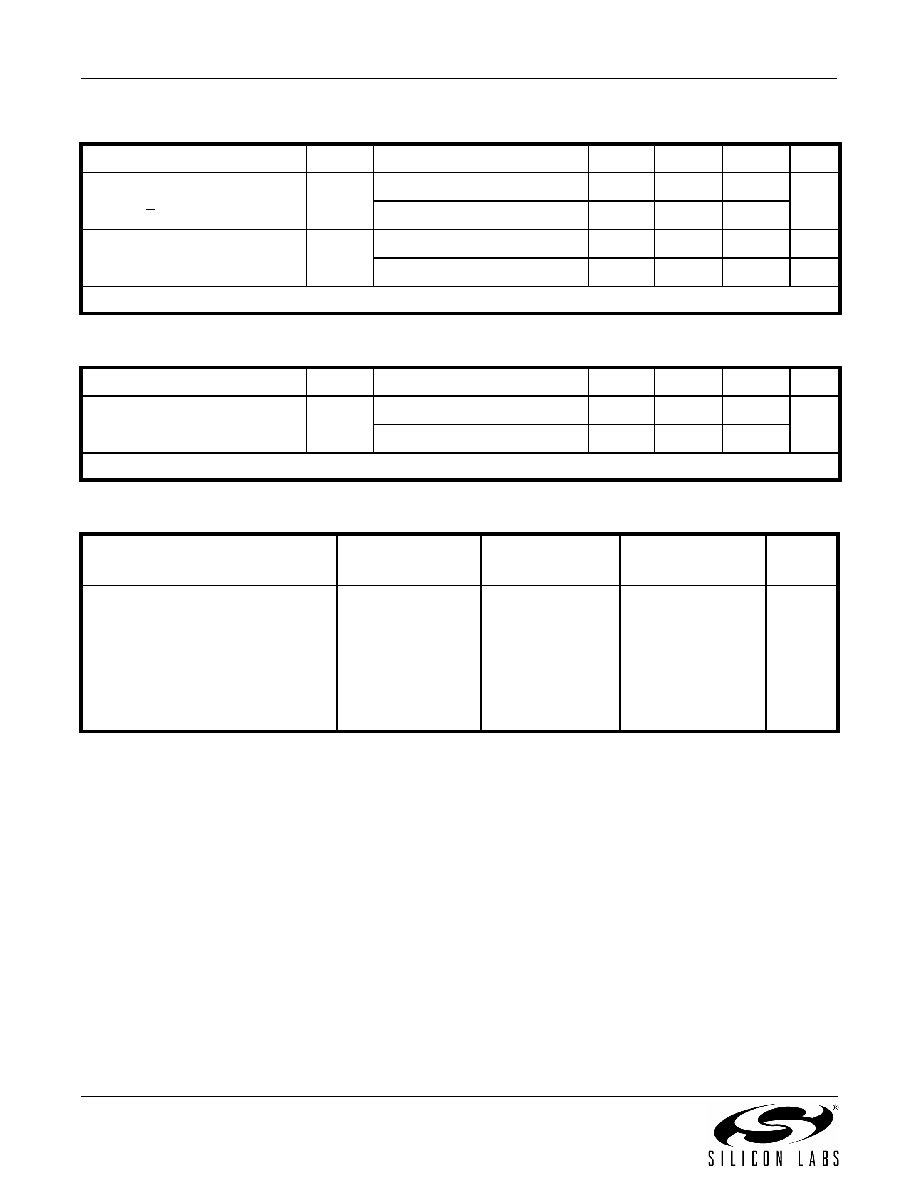
Table 4. CLK± Output Phase Jitter
Parameter
Symbol
Test Condition
Min
Typ
Max
Units
Phase Jitter (RMS)*
for FOUT > 500 MHz
φ
J
12 kHz to 20 MHz (OC-48)
—
0.25
0.40
ps
50 kHz to 80 MHz (OC-192)
—
0.26
0.37
Phase Jitter (RMS)*
for FOUT of 125 to 500 MHz
φ
J
12 kHz to 20 MHz (OC-48)
—
0.36
0.50
ps
50 kHz to 20 MHz (OC-192)
—
0.34
0.42
*Note: Differential Modes: LVPECL/LVDS/CML. Refer to AN256 for further information.
Table 5. CLK± Output Period Jitter
Parameter
Symbol
Test Condition
Min
Typ
Max
Units
Period Jitter*
JPER
RMS
—
2
—
ps
Peak-to-Peak
—
14
—
*Note: Any output mode, including CMOS, LVPECL, LVDS, CML. N = 1000 cycles. Refer to AN279 for further information.
Table 6. CLK± Output Phase Noise (Typical)
Offset Frequency (f)
120.00 MHz
LVDS
156.25 MHz
LVPECL
622.08 MHz
LVPECL
Units
100 Hz
1kHz
10 kHz
100 kHz
1MHz
10 MHz
100 MHz
–112
–122
–132
–137
–144
–150
n/a
–105
–122
–128
–135
–144
–147
n/a
–97
–107
–116
–121
–134
–146
–148
dBc/Hz
相關(guān)PDF資料 |
PDF描述 |
|---|---|
| 531FC61M0000DGR | CRYSTAL OSCILLATOR, CLOCK, 61 MHz, LVDS OUTPUT |
| 531FC622M000DGR | CRYSTAL OSCILLATOR, CLOCK, 622 MHz, LVDS OUTPUT |
| 530MA155M000DGR | CRYSTAL OSCILLATOR, CLOCK, 155 MHz, LVPECL OUTPUT |
| 530MA156M000DG | CRYSTAL OSCILLATOR, CLOCK, 156 MHz, LVPECL OUTPUT |
| 530MA209M000DGR | CRYSTAL OSCILLATOR, CLOCK, 209 MHz, LVPECL OUTPUT |
相關(guān)代理商/技術(shù)參數(shù) |
參數(shù)描述 |
|---|---|
| 531FC622M080DG | 制造商:Silicon Laboratories Inc 功能描述:SI531 2.5V LVDS, 20 PPM TOTAL, 7 PPM TEMP, 622.08 MHZ - Trays |
| 531FC622M080DGR | 制造商:Silicon Laboratories Inc 功能描述:SI531 2.5V LVDS, 20 PPM TOTAL, 7 PPM TEMP, 622.08 MHZ - Tape and Reel |
| 531FC80M0000DG | 制造商:Silicon Laboratories Inc 功能描述:XO - Trays |
| 531FC80M0000DGR | 制造商:Silicon Laboratories Inc 功能描述:OSCILLATOR - Tape and Reel |
| 531GA622M080BG | 制造商:SILABS 制造商全稱:SILABS 功能描述:CRYSTAL OSCILLATOR (XO) (10 MHZ TO 1.4 GHZ) |
發(fā)布緊急采購,3分鐘左右您將得到回復(fù)。