- 您現(xiàn)在的位置:買賣IC網(wǎng) > PDF目錄353028 > CY7C106B-25VC (CYPRESS SEMICONDUCTOR CORP) 256K x 4 Static RAM PDF資料下載
參數(shù)資料
| 型號(hào): | CY7C106B-25VC |
| 廠商: | CYPRESS SEMICONDUCTOR CORP |
| 元件分類: | DRAM |
| 英文描述: | 256K x 4 Static RAM |
| 中文描述: | 256K X 4 STANDARD SRAM, 25 ns, PDSO28 |
| 封裝: | 0.400 INCH, SOJ-28 |
| 文件頁(yè)數(shù): | 6/10頁(yè) |
| 文件大小: | 161K |
| 代理商: | CY7C106B-25VC |
CY7C106B
CY7C1006B
Document #: 38-05037 Rev. **
Page 5 of 10
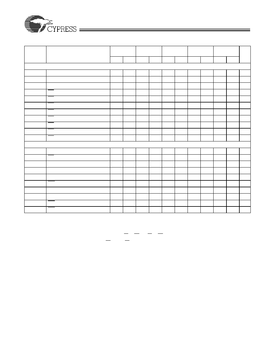
Switching Characteristics Over the Operating Range[5]
7C106B-12
7C1006B-12
7C106B-15
7C1006B-15
7C106B-20
7C1006B-20
7C106B-25
7C1006B-25
7C106B-35
Parameter
Description
Min.
Max.
Min.
Max.
Min.
Max.
Min.
Max.
Min.
Max. Unit
READ CYCLE
tRC
Read Cycle Time
12
15
20
25
35
ns
tAA
Address to Data Valid
12
15
20
25
35
ns
tOHA
Data Hold from Address Change
3
ns
tACE
CE LOW to Data Valid
12
15
20
25
35
ns
tDOE
OE LOW to Data Valid
6
7
8
10
ns
tLZOE
OE LOW to Low Z
0
ns
tHZOE
OE HIGH to High Z[6, 7]
67
8
10
ns
tLZCE
CE LOW to Low Z[7]
333
3
ns
tHZCE
CE HIGH to High Z[6, 7]
67
8
10
ns
tPU
CE LOW to Power-Up
0
ns
tPD
CE HIGH to Power-Down
12
15
20
25
35
ns
WRITE CYCLE[8, 9]
tWC
Write Cycle Time
12
15
20
25
35
ns
tSCE
CE LOW to Write End
10
12
15
20
25
ns
tAW
Address Set-Up to Write End
10
12
15
20
25
ns
tHA
Address Hold from Write End
0
ns
tSA
Address Set-Up to Write Start
0
ns
tPWE
WE Pulse Width
10
12
15
20
25
ns
tSD
Data Set-Up to Write End
7
8
10
15
20
ns
tHD
Data Hold from Write End
0
ns
tLZWE
WE HIGH to Low Z[7]
233
3
ns
tHZWE
WE LOW to High Z[6, 7]
67
8
10
ns
Notes:
5.
Test conditions assume signal transition time of 3 ns or less, timing reference levels of 1.5V, input pulse levels of 0 to 3.0V, and output loading of the specified
IOL/IOH and 30–pF load capacitance.
6.
tHZOE, tHZCE, and tHZWE are specified with a load capacitance of 5 pF as in part (b) of AC Test Loads. Transition is measured ±500 mV from steady-state voltage.
7.
At any given temperature and voltage condition, tHZCE is less than tLZCE, tHZOE is less than tLZOE, and tHZWE is less than tLZWE for any given device.
8.
The internal write time of the memory is defined by the overlap of CE and WE LOW. CE and WE must be LOW to initiate a write, and the transition of either of these
signals can terminate the write. The input data set-up and hold timing should be referenced to the leading edge of the signal that terminates the write.
9.
The minimum write cycle time for Write Cycle No. 3 (WE controlled, OE LOW) is the sum of tHZWE and tSD.
相關(guān)PDF資料 |
PDF描述 |
|---|---|
| CY7C106B-25VI | 256K x 4 Static RAM |
| CY7C106B-35VC | TV 7C 7#20 PIN RECP |
| CY7C166-20PC | 16K x 4 Static RAM |
| CY7C166-20VC | 16K x 4 Static RAM |
| CY7C166-25PC | 16K x 4 Static RAM |
相關(guān)代理商/技術(shù)參數(shù) |
參數(shù)描述 |
|---|---|
| CY7C106B-25VCT | 制造商:Rochester Electronics LLC 功能描述:- Bulk |
| CY7C106BN-15VC | 制造商:Cypress Semiconductor 功能描述: 制造商:Rochester Electronics LLC 功能描述: |
| CY7C106BN-1XW14 | 制造商:Cypress Semiconductor 功能描述:NCNR, FACT D/S ONLY, - Bulk |
| CY7C106D-10VXI | 功能描述:靜態(tài)隨機(jī)存取存儲(chǔ)器 1M 512K IND FAST ASYNC 靜態(tài)隨機(jī)存取存儲(chǔ)器 RoHS:否 制造商:Cypress Semiconductor 存儲(chǔ)容量:16 Mbit 組織:1 M x 16 訪問(wèn)時(shí)間:55 ns 電源電壓-最大:3.6 V 電源電壓-最小:2.2 V 最大工作電流:22 uA 最大工作溫度:+ 85 C 最小工作溫度:- 40 C 安裝風(fēng)格:SMD/SMT 封裝 / 箱體:TSOP-48 封裝:Tray |
| CY7C106D-10VXIT | 功能描述:靜態(tài)隨機(jī)存取存儲(chǔ)器 1M 512K IND FAST ASYNC 靜態(tài)隨機(jī)存取存儲(chǔ)器 RoHS:否 制造商:Cypress Semiconductor 存儲(chǔ)容量:16 Mbit 組織:1 M x 16 訪問(wèn)時(shí)間:55 ns 電源電壓-最大:3.6 V 電源電壓-最小:2.2 V 最大工作電流:22 uA 最大工作溫度:+ 85 C 最小工作溫度:- 40 C 安裝風(fēng)格:SMD/SMT 封裝 / 箱體:TSOP-48 封裝:Tray |
發(fā)布緊急采購(gòu),3分鐘左右您將得到回復(fù)。