- 您現(xiàn)在的位置:買賣IC網(wǎng) > PDF目錄256062 > BUS-65154-190Q (DATA DEVICE CORP) 2 CHANNEL(S), 1M bps, MIL-STD-1553 CONTROLLER, CQIP70 PDF資料下載
參數(shù)資料
| 型號(hào): | BUS-65154-190Q |
| 廠商: | DATA DEVICE CORP |
| 元件分類: | 微控制器/微處理器 |
| 英文描述: | 2 CHANNEL(S), 1M bps, MIL-STD-1553 CONTROLLER, CQIP70 |
| 封裝: | 1.900 X 1 INCH, 0.215 INCH HEIGHT, CERAMIC, DIP-70 |
| 文件頁(yè)數(shù): | 24/40頁(yè) |
| 文件大?。?/td> | 349K |
| 代理商: | BUS-65154-190Q |
第1頁(yè)第2頁(yè)第3頁(yè)第4頁(yè)第5頁(yè)第6頁(yè)第7頁(yè)第8頁(yè)第9頁(yè)第10頁(yè)第11頁(yè)第12頁(yè)第13頁(yè)第14頁(yè)第15頁(yè)第16頁(yè)第17頁(yè)第18頁(yè)第19頁(yè)第20頁(yè)第21頁(yè)第22頁(yè)第23頁(yè)當(dāng)前第24頁(yè)第25頁(yè)第26頁(yè)第27頁(yè)第28頁(yè)第29頁(yè)第30頁(yè)第31頁(yè)第32頁(yè)第33頁(yè)第34頁(yè)第35頁(yè)第36頁(yè)第37頁(yè)第38頁(yè)第39頁(yè)第40頁(yè)
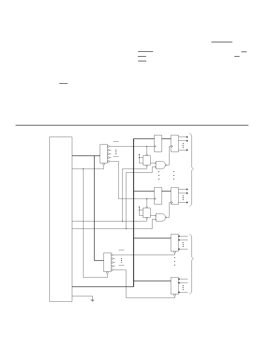
SIMPLE SYSTEM INTERFACE
FIGURE 16 illustrates the capability of the STIC to operate in a
system with no host processor. A simple linear addressing
scheme is used that can be easily decoded to form read and
write signals for direct access to data buffers or data latches. A
double buffered mechanism may be used on received data in
order to maintain data validity and consistency.
The latched discrete outputs section of the drawing uses two
sets of latches. The first latch is updated when the received data
word is transferred from the STIC. The second latch is not updat-
ed until the message is validated, as indicated by the signal
Good Block Received (GBR). If an error, such as parity or
Manchester, occurs on a received data word, all the data asso-
ciated with that message will be ignored, thus fulfilling the data
validity/consistancy requirement.
DMA INTERFACE
The STIC may be interfaced to a host processor by means of a
simple DMA interface. The address and control lines may be
placed in a three-state mode by setting the ADDR_ENA signal to
logic “1”. While the STIC is not accessing the RAM (i.e.,
DT_ACK is logic “1”) the address, data, and control lines (CS,
WRT) are held in a high impedance state. The signals CS and
WRT require pull-up resistors.
The STIC may be programmed to operate in either a 16-bit
transfer mode (FIGURE 17) or an 8-bit transfer mode (FIGURE
18). In 16-bit mode (DB_SEL set to logic “0”) the signal A0 is not
used (always logic “1”) and 16-bit transfers are performed on
data lines D0..D15. In 8-bit mode (DB_SEL set to logic “1”) the
signal A0 is used to indicate whether the upper (MSB) data byte
(A0 set to logic “1”) or the lower (LSB) data byte (A0 set to logic
“0”) is being transferred. The upper and lower data bytes are not
multiplexed internally, therefore, the signals must be connected
externally. D0 must be connected to D8, D1 must be connected
to D9, ... , and D7 must be connected to D15
30
FIGURE 16. BUS-65153 MINIMUM COMPLEXITY SYSTEM
Q
LATCH
DQ
D
W0
WRITE
ADDRESS
DECODER
CS
A0..A13
__
WN
Vcc
D
Q
_
Q
LATCHED
DISCRETE
OUTPUTS
Q
LATCH
DQ
D
BUS
65153
"STIC"
Vcc
D
_
Q
TRI-STATE
BUFFER
Q
NBGRT
GBR
_____
___
ADDRESS
DECODER
READ
R0
DISCRETE
BUFFERED
INPUTS
TRI-STATE
BUFFER
RN
DB GRT
DB0..DB15
______
相關(guān)PDF資料 |
PDF描述 |
|---|---|
| BUS-65163-180K | 2 CHANNEL(S), 1M bps, MIL-STD-1553 CONTROLLER, CDFP70 |
| BU-61743F3-262 | 2 CHANNEL(S), 1M bps, MIL-STD-1553 CONTROLLER, CQFP72 |
| BU-61743F3-300Q | 2 CHANNEL(S), 1M bps, MIL-STD-1553 CONTROLLER, CQFP72 |
| BU-61743F3-432Z | 2 CHANNEL(S), 1M bps, MIL-STD-1553 CONTROLLER, CQFP72 |
| BU-61743F3-490L | 2 CHANNEL(S), 1M bps, MIL-STD-1553 CONTROLLER, CQFP72 |
相關(guān)代理商/技術(shù)參數(shù) |
參數(shù)描述 |
|---|---|
| BU-S802 | 制造商:Fuji Electric 功能描述: |
| BU-S803 | 制造商:Fuji Electric 功能描述: |
| BUS98 | 制造商:ONSEMI 制造商全稱:ON Semiconductor 功能描述:SITCHMODE Series NPN Silicon Power Transistors |
| BUS98/D | 制造商:未知廠家 制造商全稱:未知廠家 功能描述:SWITCHMODE? Series NPN Silicon Power Transistors |
| BUS98A | 制造商:ONSEMI 制造商全稱:ON Semiconductor 功能描述:SITCHMODE Series NPN Silicon Power Transistors |
發(fā)布緊急采購(gòu),3分鐘左右您將得到回復(fù)。