- 您現(xiàn)在的位置:買賣IC網(wǎng) > PDF目錄366551 > AM79C989 (Advanced Micro Devices, Inc.) Motor Driver IC; Supply Voltage Max:13.2V; Output Current Max:0.5A; Package/Case:8-SOIC; Driver Type:Motor; Leaded Process Compatible:No; Output Current:1.5A; Peak Reflow Compatible (260 C):No; Supply Voltage Min:3.8V PDF資料下載
參數(shù)資料
| 型號: | AM79C989 |
| 廠商: | Advanced Micro Devices, Inc. |
| 元件分類: | 基準(zhǔn)電壓源/電流源 |
| 英文描述: | Motor Driver IC; Supply Voltage Max:13.2V; Output Current Max:0.5A; Package/Case:8-SOIC; Driver Type:Motor; Leaded Process Compatible:No; Output Current:1.5A; Peak Reflow Compatible (260 C):No; Supply Voltage Min:3.8V |
| 中文描述: | 四路以太網(wǎng)交換器(QuEST的⑩) |
| 文件頁數(shù): | 17/37頁 |
| 文件大?。?/td> | 198K |
| 代理商: | AM79C989 |
第1頁第2頁第3頁第4頁第5頁第6頁第7頁第8頁第9頁第10頁第11頁第12頁第13頁第14頁第15頁第16頁當(dāng)前第17頁第18頁第19頁第20頁第21頁第22頁第23頁第24頁第25頁第26頁第27頁第28頁第29頁第30頁第31頁第32頁第33頁第34頁第35頁第36頁第37頁
Am79C989
17
P R E L I M I N A R Y
QRX_CRS signal is primarily useful for calibrating net-
work timers in the external MAC or repeater device.
Data which is held in the elasticity FIFO will be delayed.
When the QRX_VALID (Receive Data Valid) is
asserted in the appropriate slot, the QRX_DATA is
valid. QRX_VALID is used as a framing signal to indi-
cate when the QRX_DATA is valid. QRX_VALID and
QRX_DATA will lag QRX_CRS by up to four bit times
(400 ns) in the beginning of the frame and up to 8 bits
by the end of the frame. The reason that QRX_VALID
lags QRX_CRS signal by a variable amount of time is
due to the inherent rate mismatch between the
received data and network clocks.
The QCLSN signal is asserted whenever a network
collision is detected. QCLSN is time multiplexed like the
other receive signals. QCLSN has a specific meaning
within the specified channel or slot number. Collision
indication is asserted in its appropriate time slot when-
ever a network collision is detected. The QCLSN pin
may be optionally asserted if the SQE_TEST disable
bit, Control Register (Reg. 18, bit 0), is in a cleared
state after transmission of a packet.
In summary, the QuASI Interface is synchronous to the
clock input, SCLK. A reset signal, QRST/STRB, is pro-
vided which serves two purposes, hardware reset and
a means for channel slot synchronization. There are six
additional signal pins that communicate the serial data
to and from the QuEST device.
Management Interface
The QuEST device incorporates a two-wire Manage-
ment Interface in conformance with the MII Manage-
ment Interface of the IEEE 802.3u Standard. The
interface includes a management clock, MDC, and a
serial data I/O pin, MDIO. The Management Interface
clock can operate as high as 20 MHz; there is no lower
frequency limit. The MDIO signal serves as both con-
trol and data. The first part of the command is com-
posed of control information, while the second half is
composed of data. The management frame format is
indicated below.
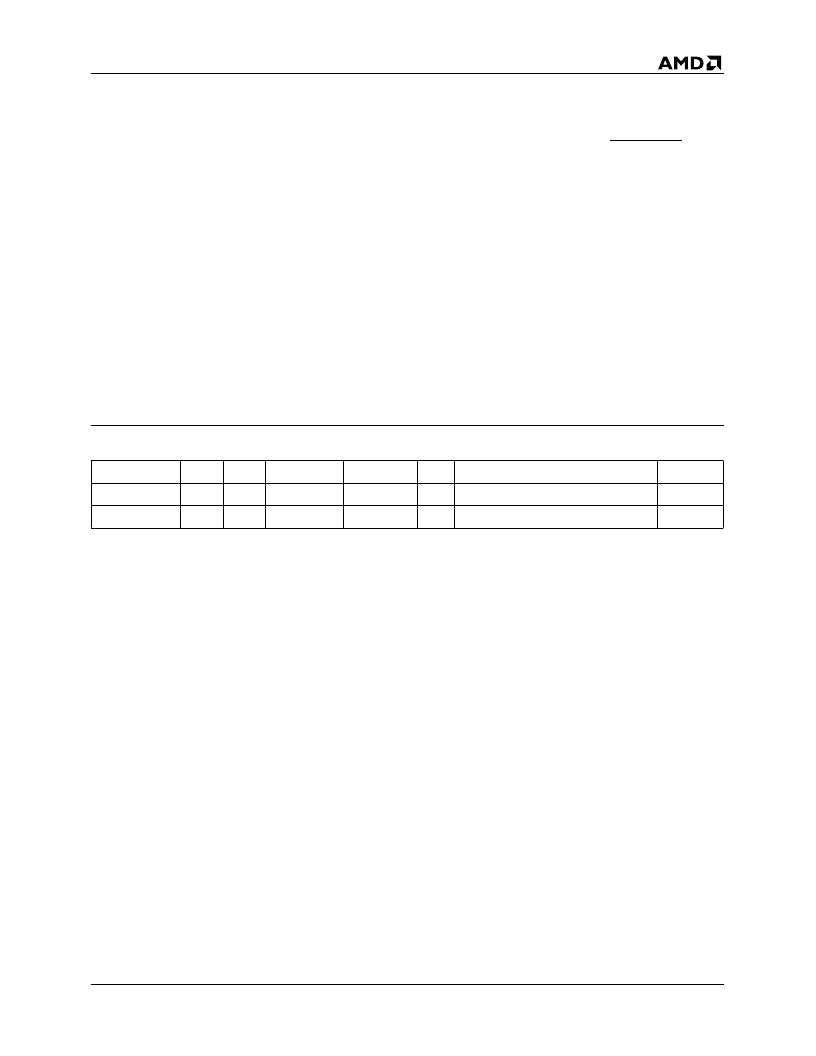
Table 1.
Management Frame Fields
The Management Frame
The management frame begins with the Start of Frame
(ST) delimiter indicated by a <01> pattern. After the ST
pattern, the Operation Code (OP) indicates either a
read or a write, followed by the PHYAD and REGAD
fields. The specific address is identified by the five bits
of the PHY address (PHYAD); the specific register is
identified by the five bits of the Register Address (RE-
GAD). The Turn Around (TA) field follows and provides
a two-cycle delay for redirecting the MDIO bus during
read commands, to avoid signal contention. The man-
agement frame includes the 16-bit wide data field and
terminates with an idle state indication.
PHY Addressing
PHYAD is the unique address of any PHY connected to
this Serial Management Interface. Each QuEST sup-
ports four PHYs, and up to eight QuEST devices can
be connected to the Management Interface. A total of
32 PHYs can be managed. (Refer to Table 2.)
The internal QuEST address is formed through exter-
nal means. During reset, the QRX_DATA, QRX_VALID,
QRX_CRS, and QCLSN signals of the QuEST device
are in tristate. At the rising edge of reset, the QuEST
device latches signal pins QRX_VALID, QRX_CRS,
and QCLSN to form the internal address which the
QuEST device will use to match against. The QuEST
device provides internal pull-down resistors of approxi-
mately 100 k
.
Pull-up resistors of 10 k
in value can be placed on the
QRX_DATA, QRX_VALID, and QCLSN signals to de-
fine the internally latched address. The internal latch
address is shown below. The internally latched address
must be unique among QuEST devices shared by a
single Management Interface. To form the QuEST ad-
dress “000,” no resistors need to be connected. To form
the QuEST address “101”, external pull-up resistors
are required to be added to the QRX_DATA and
QCLSN signals, and so forth.
A specific PHY address (PHYAD) is formed with five
bits. The upper three bits of the PHYAD, A4, A3, and
A2, are matched to an internal QuEST device address
which acts as a chip selection function. Setting each of
these three bits to 0 or 1 in combination allows specific
designation of up to eight QuEST devices. The lower
two bits of the PHYAD designate the channel number
of the designated QuEST device.
ST
OP
PHYAD
REGAD
TA
DATA
IDLE
READ
01
10
A
4
AAAA
0
R
4
RRRR
0
Z0
D
15
DDDDDDDDDDDDDDD
0
Z
WRITE
01
01
A
4
AAAA
0
R
4
RRRR
0
10
D
15
DDDDDDDDDDDDDDD
0
Z
相關(guān)PDF資料 |
PDF描述 |
|---|---|
| AM79C989JC | Quad Ethernet Switching Transceiver (QuEST⑩) |
| AM79C989JCT | Quad Ethernet Switching Transceiver (QuEST⑩) |
| AM79C98 | Twisted-Pair Ethernet Transceiver (TPEX) |
| AM79C98JC | Twisted-Pair Ethernet Transceiver (TPEX) |
| AM79C98PC | Twisted-Pair Ethernet Transceiver (TPEX) |
相關(guān)代理商/技術(shù)參數(shù) |
參數(shù)描述 |
|---|---|
| AM79C989JC | 制造商:Rochester Electronics LLC 功能描述:- Bulk |
| AM79C989JC/T | 制造商:Rochester Electronics LLC 功能描述:- Bulk |
| AM79C989JCT | 制造商:AMD 制造商全稱:Advanced Micro Devices 功能描述:Quad Ethernet Switching Transceiver (QuEST⑩) |
| AM79C98JC | 制造商:AMD 制造商全稱:Advanced Micro Devices 功能描述:Twisted-Pair Ethernet Transceiver (TPEX) |
發(fā)布緊急采購,3分鐘左右您將得到回復(fù)。