- 您現(xiàn)在的位置:買賣IC網(wǎng) > PDF目錄378283 > ADC12138 (National Semiconductor Corporation) Self-Calibrating 12-Bit Plus Sign Serial I/O A/D Converters with MUX and Sample/Hold PDF資料下載
參數(shù)資料
| 型號(hào): | ADC12138 |
| 廠商: | National Semiconductor Corporation |
| 元件分類: | 串行ADC |
| 英文描述: | Self-Calibrating 12-Bit Plus Sign Serial I/O A/D Converters with MUX and Sample/Hold |
| 中文描述: | 自校準(zhǔn)12位帶符號(hào)串行I /辦公自動(dòng)化/ D轉(zhuǎn)換器MUX和采樣/保持 |
| 文件頁(yè)數(shù): | 35/41頁(yè) |
| 文件大小: | 1085K |
| 代理商: | ADC12138 |
第1頁(yè)第2頁(yè)第3頁(yè)第4頁(yè)第5頁(yè)第6頁(yè)第7頁(yè)第8頁(yè)第9頁(yè)第10頁(yè)第11頁(yè)第12頁(yè)第13頁(yè)第14頁(yè)第15頁(yè)第16頁(yè)第17頁(yè)第18頁(yè)第19頁(yè)第20頁(yè)第21頁(yè)第22頁(yè)第23頁(yè)第24頁(yè)第25頁(yè)第26頁(yè)第27頁(yè)第28頁(yè)第29頁(yè)第30頁(yè)第31頁(yè)第32頁(yè)第33頁(yè)第34頁(yè)當(dāng)前第35頁(yè)第36頁(yè)第37頁(yè)第38頁(yè)第39頁(yè)第40頁(yè)第41頁(yè)
Application Hints
(Continued)
11.0 CLOCK SIGNAL LINE ISOLATION
The ADC12130/2/8’s performance is optimized by routing
the analog input/output and reference signal conductors as
far as possible from the conductors that carry the clock sig-
nals to the CCLK and SCLK pins. Ground traces parallel to
the clock signal traces can be used on printed circuit boards
to reduce clock signal interference on the analog input/
output pins.
12.0 THE CALIBRATION CYCLE
A calibration cycle needs to be started after the power sup-
plies, reference, and clock have been given enough time to
stabilize after initial turn-on. During the calibration cycle, cor-
rection values are determined for the offset voltage of the
sampled data comparator and any linearity and gain errors.
These values are stored in internal RAM and used during an
analog-to-digital conversion to bring the overall full-scale,
offset, and linearity errors down to the specified limits.
Full-scale error typically changes
±
0.4 LSB over tempera-
ture and linearity error changes even less; therefore it should
be necessary to go through the calibration cycle only once
after power up if the Power Supply Voltage and the ambient
temperature do not change significantly (see the curves in
the Typical Performance Characteristics).
13.0 THE AUTO-ZERO CYCLE
To correct for any change in the zero (offset) error of theA/D,
the auto-zero cycle can be used. It may be necessary to do
an auto-zero cycle whenever the ambient temperature or the
power supply voltage change significantly. (See the curves
titled “Zero Error Change vs Ambient Temperature” and
“Zero Error Change vs Supply Voltage” in the Typical Perfor-
mance Characteristics.)
14.0 DYNAMIC PERFORMANCE
Many applications require the A/D converter to digitize AC
signals, but the standard DC integral and differential nonlin-
earity specifications will not accurately predict the A/D con-
verter’s performance with AC input signals. The important
specifications for AC applications reflect the converter’s abil-
ity to digitize AC signals without significant spectral errors
and without adding noise to the digitized signal. Dynamic
characteristics such as signal-to-noise (S/N), signal-to-noise
+ distortion ratio (S/(N + D)), effective bits, full power band-
width, aperture time and aperture jitter are quantitative mea-
sures of the A/D converter’s capability.
An A/D converter’s AC performance can be measured using
Fast Fourier Transform (FFT) methods. A sinusoidal wave-
form is applied to the A/D converter’s input, and the trans-
form is then performed on the digitized waveform. S/(N + D)
and S/N are calculated from the resulting FFT data, and a
spectral plot may also be obtained. Typical values for S/N
are shown in the table of Electrical Characteristics, and
spectral plots of S/(N + D) are included in the typical perfor-
mance curves.
The A/D converter’s noise and distortion levels will change
with the frequency of the input signal, with more distortion
and noise occurring at higher signal frequencies. This can be
seen in the S/(N + D) versus frequency curves. These curves
will also give an indication of the full power bandwidth (the
frequency at which the S/(N + D) or S/N drops 3 dB).
Effective number of bits can also be useful in describing the
A/D’s noise performance. An ideal A/D converter will have
some amount of quantization noise, determined by its reso-
lution, which will yield an optimum S/N ratio given by the fol-
lowing equation:
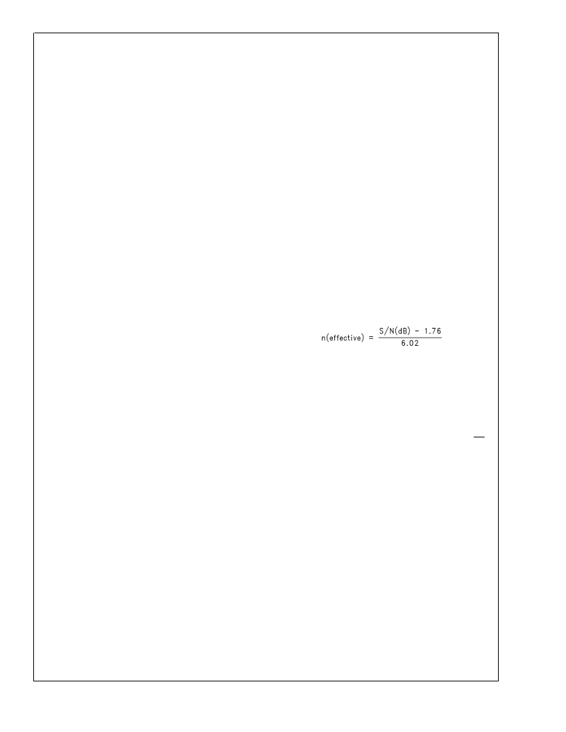
S/N = (6.02 x n + 1.76) dB
where n is the A/D’s resolution in bits.
The effective bits of a real A/D converter, therefore, can be
found by:
As an example, this device with a differential signed 5V,
10 kHz sine wave input signal will typically have a S/N of
78 dB, which is equivalent to 12.6 effective bits.
15.0 AN RS232 SERIAL INTERFACE
Shown on the following page is a schematic for an RS232 in-
terface to any IBM and compatible PCs. The DTR, RTS, and
CTS RS232 signal lines are buffered via level translators
and connected to the ADC12138’s DI, SCLK, and DO pins,
respectively. The D flip/flop is used to generate the CS
signal.
A
www.national.com
35
相關(guān)PDF資料 |
PDF描述 |
|---|---|
| ADC12130CIN | Self-Calibrating 12-Bit Plus Sign Serial I/O A/D Converters with MUX and Sample/Hold |
| ADC12130CIWM | Self-Calibrating 12-Bit Plus Sign Serial I/O A/D Converters with MUX and Sample/Hold |
| ADC12138CIMSA | Self-Calibrating 12-Bit Plus Sign Serial I/O A/D Converters with MUX and Sample/Hold |
| ADC12138CIN | Self-Calibrating 12-Bit Plus Sign Serial I/O A/D Converters with MUX and Sample/Hold |
| ADC12181 | 12-Bit, 10 MHz Self-Calibrating, Pipelined A/D Converter with Internal Sample & Hold |
相關(guān)代理商/技術(shù)參數(shù) |
參數(shù)描述 |
|---|---|
| ADC12138CIMSA | 功能描述:模數(shù)轉(zhuǎn)換器 - ADC RoHS:否 制造商:Texas Instruments 通道數(shù)量:2 結(jié)構(gòu):Sigma-Delta 轉(zhuǎn)換速率:125 SPs to 8 KSPs 分辨率:24 bit 輸入類型:Differential 信噪比:107 dB 接口類型:SPI 工作電源電壓:1.7 V to 3.6 V, 2.7 V to 5.25 V 最大工作溫度:+ 85 C 安裝風(fēng)格:SMD/SMT 封裝 / 箱體:VQFN-32 |
| ADC12138CIMSA/NOPB | 功能描述:模數(shù)轉(zhuǎn)換器 - ADC SELF-CALIBR 12B PLUS SIGN SERIAL I/O ADC RoHS:否 制造商:Texas Instruments 通道數(shù)量:2 結(jié)構(gòu):Sigma-Delta 轉(zhuǎn)換速率:125 SPs to 8 KSPs 分辨率:24 bit 輸入類型:Differential 信噪比:107 dB 接口類型:SPI 工作電源電壓:1.7 V to 3.6 V, 2.7 V to 5.25 V 最大工作溫度:+ 85 C 安裝風(fēng)格:SMD/SMT 封裝 / 箱體:VQFN-32 |
| ADC12138CIMSANOPB | 制造商:TI 功能描述:Pb Free |
| ADC12138CIMSAX | 功能描述:模數(shù)轉(zhuǎn)換器 - ADC RoHS:否 制造商:Texas Instruments 通道數(shù)量:2 結(jié)構(gòu):Sigma-Delta 轉(zhuǎn)換速率:125 SPs to 8 KSPs 分辨率:24 bit 輸入類型:Differential 信噪比:107 dB 接口類型:SPI 工作電源電壓:1.7 V to 3.6 V, 2.7 V to 5.25 V 最大工作溫度:+ 85 C 安裝風(fēng)格:SMD/SMT 封裝 / 箱體:VQFN-32 |
| ADC12138CIMSAX/NOPB | 功能描述:模數(shù)轉(zhuǎn)換器 - ADC RoHS:否 制造商:Texas Instruments 通道數(shù)量:2 結(jié)構(gòu):Sigma-Delta 轉(zhuǎn)換速率:125 SPs to 8 KSPs 分辨率:24 bit 輸入類型:Differential 信噪比:107 dB 接口類型:SPI 工作電源電壓:1.7 V to 3.6 V, 2.7 V to 5.25 V 最大工作溫度:+ 85 C 安裝風(fēng)格:SMD/SMT 封裝 / 箱體:VQFN-32 |
發(fā)布緊急采購(gòu),3分鐘左右您將得到回復(fù)。